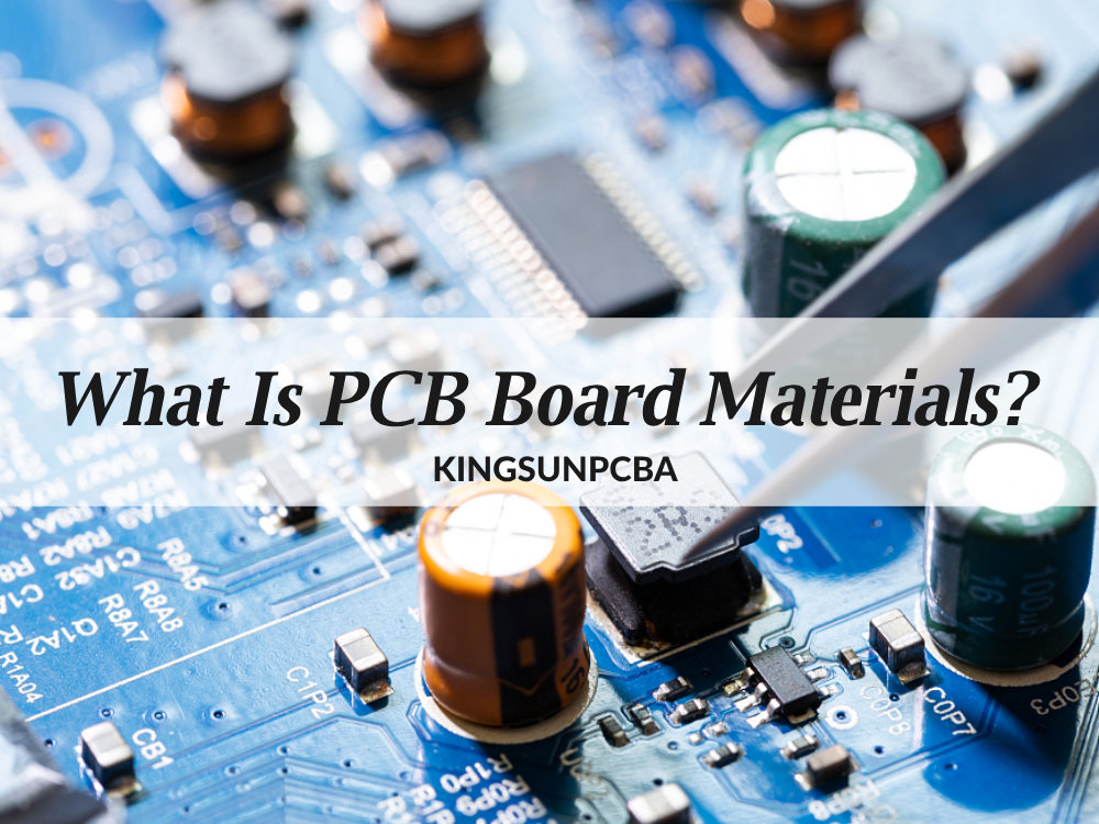
Entdecken Sie die wichtigsten Materialien, die bei der Herstellung von Leiterplatten (PCBs) verwendet werden. Erfahren Sie mehr über FR-4, Leiterplatten mit Metallkern, flexible Leiterplattenmaterialien und mehr. Entdecken Sie die Vorteile und Anwendungen verschiedener Leiterplattenmaterialien für Ihre Anforderungen an das elektronische Design.
Keramische Leiterplatten bestehen eigentlich aus elektronischen Keramikmaterialien und können in verschiedene Formen gebracht werden. Unter ihnen weist die keramische Leiterplatte die Eigenschaften einer hohen Temperaturbeständigkeit und einer hohen elektrischen Isolationsleistung auf und hat die Vorteile einer niedrigen Dielektrizitätskonstante, eines geringen dielektrischen Verlusts, einer hohen Wärmeleitfähigkeit, einer guten chemischen Stabilität und einer ähnlichen Wärmeausdehnung …
In the design of the circuit board, with the rapid increase of frequency, there will be many interferences different from the design of the low frequency PCB. As the frequency increases and the contradiction between the miniaturization and cost reduction of PCB boards becomes more and more prominent, these interferences are more and more complicated. In…
PCB raw materials will continue to increase in price in 2021 PCB raw materials include copper foil, fiberglass, resin and other related materials have been reported of price adjustments in Q1 of 2021.Recently, from CCL factory to PCB factory, we have received notices about product price increase.Even PCB industry has fired the first shot, pointing out that the…
18
September
September
The PCB ground plane is akin to the foundation of a skyscraper, providing stability, structure, and a solid reference point for the entire circuit. It is the unobtrusive conductor that silently conducts return currents, guards against electronic interference, and maintains voltage reference levels. In this article, we delve into the fascinating world of PCB ground planes, exploring their significance, functions, and the pivotal role they play in modern electronics.
18
September
September
Do you know the advantages of PCB pouring copper on the surface of the PCB? In the whole process of PCB design, engineers want to ignore the link of pouring copper on the bottom of the PCB in order to save time. Is this right? Is it necessary for the PCB to pouring copper on the bottom of the surface? What are the…
18
September
September
The process of testing PCB circuit boards is a critical step in the manufacturing and assembly of electronic devices. It involves a series of meticulously designed evaluations and assessments to confirm that the PCB functions as intended and is free from defects. These tests not only assure the quality of the final product but also play a crucial role in identifying and rectifying issues early in the production process.
With the rapid development of electronic design technology and manufacturing technology, electronic products are gradually developing towards high density, high functionality, light,small, and high transmission rate; In addition, with the rapid development of chip miniaturization and the increase of the number of data transmission, the working frequency of the system is higher and higher, and…
When the PCB design is completed, the laminate layer is determined, and the PCB board has been put into fabrication, the simulation evaluation found that the high-speed signal channel margin may be unsafe. Is there still a chance to improve? Let’s first introduce the loss classification of PCB. There are three kinds of losses: conductor…
How to choose how many layers of boards are used for design and how to stack them, Today we are going to talk about this topic. The following are some common stacked structures, let’s analyze them: PCB Layer stackup of single-sided and double-sided boards For two-layer boards, there is no stacking problem due to the small…