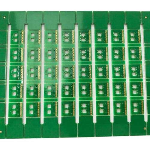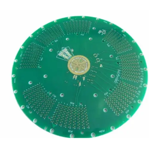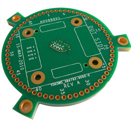
Via in Pad PCB Prototype:
Schichten: 4 Schichten
Leiterplattenmaterial: FR4
Board Thickness: 1.2mm
Surface Finishing: Hard Gold
Finished Copper thickness:1/1/1/1 OZ
Sonderverfahren:
- Gold Thickness 20u”
- Depth Milling
- Via in Pad
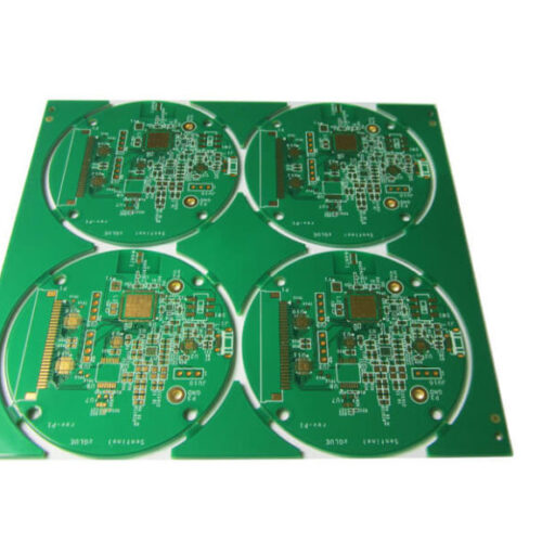
HDI&Microvia(blind buried) PCB Capability:
| Minimale Leiterbahnbreite/-abstand: 2,7/2,7mil |
| The Minimum Via Size: 0.1mm |
| Minimale Legendenhöhe/-breite: 0,5 mm/0,12 mm |
| Surface Finishing: HASL-LF, ENIG, ENEPIG, OSP, Gold Finger, Hard Gold Plating, Immersion Silver, Immersion Tin |
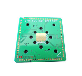
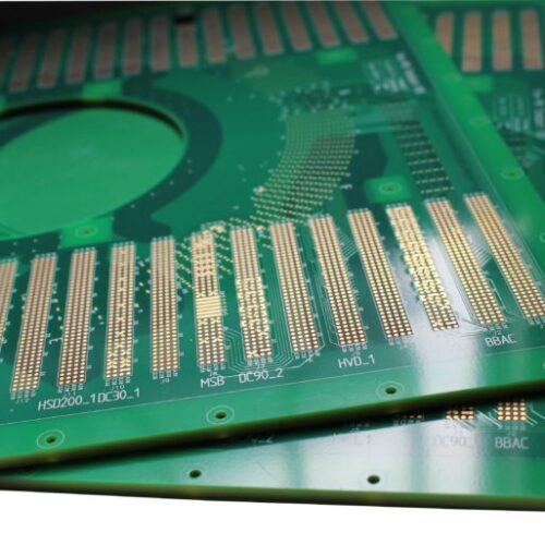
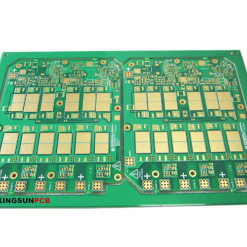
| Special Technology: Blind&buried via, Via In Pad, Backdrill,Small BGA Pad, Impedance control, Heavy Copper, Copper Filled Vias, Countersink hole, Depth Milling |
| Materialtyp: FR4, Metallkern, halogenfreies FR4, Rogers, PTFE, Arlon, Nelco, Polyimid |
| Maximale Plattenabmessung: 1200 mm x 600 mm |
| Endgültige Plattendicke: 0,4 mm – 6,0 mm |
| Endgültige Kupferdicke: HOZ 1OZ 2OZ 3OZ 4OZ 6OZ 10OZ |
| Dicke des FR4-Substrats: 0,1 mm 0,2 mm 0,3 mm 0,4 mm 0,5 mm 0,6 mm 0,8 mm 1,0 mm 1,2 mm 1,5 mm 2,0 mm 2,36 mm |
| Solder Mask Colour: Green, White Black Red Blue Yellow |
| Shaping: CNC Routing, Punching, V-CUT, Depth milling, Castellation |
| Special Hole: Blind&buried hole, Depth milling, T-slot, Countersink hole |