Für ein leistungsstarkes Design ist es von entscheidender Bedeutung, PCB-Vias zu verstehen, die wesentlichen Elemente zum Verbinden von Schichten innerhalb einer Leiterplatte.
In diesem Handbuch werden Grundlagen wie Pad- und Bohrgrößen sowie Herstellerfunktionen behandelt. Wir untersuchen Strategien zur Platzierung von Vias, um die Induktivität zu minimieren, die Montage zu verbessern und Hohlräume zu vermeiden. Wir behandeln auch das Zusammenfügen von PCB-Vias zu Abschirmungszwecken.
Was ist eine Via?
We all know traces are connections on a plane. So, on a layer, we can route anywhere on that plane, usually called a trace. Or we can use things such as copper pours.
However, we must use a via once we want to route between layers, such as connecting layer one to layer three.
Essentially, it’s just a vertical connection in the third dimension. It is used for connections between layers, so our trace on one layer can jump to any or multiple layers in a PCB. We don’t just have to end up on one layer.
If we’re not connecting to a specific layer via a link, we will create a void on that layer, and we’ll look at that in more detail later.
Arten von Durchkontaktierungen
Leiterplatten sind mit Kupferfolien-Schaltungsschichten gestapelt, wobei Durchkontaktierungen die verschiedenen Schaltungsschichten verbinden. Die Bohrkosten können bis zu 301-401 TP3T der gesamten Platine betragen.
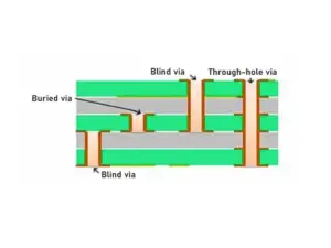
Durchkontaktierte Löcher (PTH), Sacklöcher (BVH) und vergrabene Löcher (BVH) sind die Standardtypen bei Durchkontaktierungen im PCB-Design. Die Details dieser drei Typen von Substrat-Durchkontaktierungen sind unten dargestellt.
Durchkontaktierte Bohrung (PTH)
Plated through-holes are the most common PCB vias. If you face the board to the light and see the light, it’s a “through hole.” Incorporating a laser will significantly assist you in making a complete borehole.
Furthermore, the cost will be relatively low. However, in some cases, no through holes are required. It’s cheaper, but it may need more board space.
There are usually two types of through holes: PTH and NPTH. The difference between the two is whether it has copper or not.
PTH holes do not have copper and are often used for inserting electronic components (the hole diameter is slightly larger). It is also used to connect patterns on the inner and outer layers.
Blind Beer Hall (BVH)
Unlike through-hole vias that pass entirely through the PCB, blind vias connect the outermost layer and a single, specific inner layer.
Since the via doesn’t emerge on the opposite side of the board, it’s called a “blind path.” This technique allows for more efficient use of space on the PCB’s surface.
This manufacturing method requires attention to the hole depth (Z-axis). Because hole plating is complex, only some board manufacturers use this method.
Vergrabenes Via-Hole (BVH)
A buried via hole is a hole that connects to any circuit layer on the board without passing through the outer layer.
This process cannot be carried out using the method of drilling and bonding but requires the drilling process to be made into individual circuit layers, followed by plating and then lamination pressing, which are repeated in three steps.
It takes longer to manufacture than “through hole” and “blind via hole,” and its price is the highest.
HDI PCBs often incorporate blind vias to maximize space for additional circuit layers. Besides drill sizes, pad sizes, and annular rings, many other parameters make up a via.
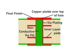
For example, PCB via tenting, which covers the via with the solder mask, typically costs no extra; filling the via will be additional.
Was sind die Unterschiede zwischen den verschiedenen Via-Typen?
One can be sure through-hole vias were made with a drill. Different drill sizes are used, but generally, nothing less than 0.2 mm is used. They go up from there to very much bigger ones.
The drills make the holes under digital control using numerically controlled machines.
As a general rule, multi-spindle tools are used. Subsequently, the tiny holes are made in batches, one after the other. It takes a finite time, and linear motors control the spindles. They turn relatively fast to achieve a good hole quality.
Funktionalität von Vias
Wenn wir über Vias sprechen, gibt es bestimmte Hauptparameter. PCB-Vias sind entscheidend für die Beschleunigung komplexer Funktionen auf einer mehrschichtigen Leiterplatte. Lassen Sie uns jeden einzelnen näher betrachten:
Signalführung:
Without through-hole vias, signals could not travel from one layer of the PCB to another. Vias’ role is similar to that of electrical lifts, as they help provide interconnection between different layers. Therefore, this allows the designers to have complex networks and ensure fast signals are effectively transmitted.
Strom- und Erdungsverteilung:
Durchkontaktierungen sind für die Strom- und Erdungsversorgung der gesamten Leiterplatte von entscheidender Bedeutung. Sie verbinden Strom- und Erdungsebenen auf verschiedenen Ebenen. Dadurch gewährleisten sie eine stabile und konstante Spannungsversorgung aller Komponenten. Darüber hinaus minimieren Leiterplattendurchkontaktierungen Spannungsabfälle und gewährleisten die Signalintegrität.
Fluchtweglenkung:
Bei der Oberflächenmontagetechnik (SMT) gibt es Anschlüsse. Diese Anschlüsse müssen mit internen Schichten verbunden werden. Vias, insbesondere Durchgangslöcher, bieten einen Fluchtweg für diese Verbindungen.
Welche Regeln gelten für das Routing einer Leiterplatte?
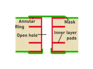
Dies ist sehr wichtig. Lassen Sie uns über die Routing-Regeln für Durchgangslöcher sprechen. Gemäß den IPC-Standards muss ein Loch auf dem Pad zentriert sein. Gemäß IPC und ISO ist ein Loch tangential zum Pad zulässig, aber das Leiterplattenmaterial kann sich bewegen und Maschinen haben eine Toleranz. Aus diesen Gründen muss das Pad größer als der Lochdurchmesser sein.
If you take the example of a pad of 0.55 mm, you can drill a hole of 0.3 mm. This will give us a finished hole between 0.2 and 0.25 mm, which is relatively small. Similarly, in this case, we must allow isolation on the internal layers of the order of 750 µ if we don’t want a connection.
Außerdem benötigen wir außen eine zentrale Öffnung im Lack von etwa 450 µ. Das ist etwa die Hälfte des Bohrdurchmessers. Was Laser-Mikro-Vias betrifft, ist auf der Ebene des PCB-Designs ein Pad von 300 µ der Standard. Hier beträgt das fertige Loch etwa 100 µ. In diesem Fall können wir etwas enger gehen, bis auf ein Minimum von 275. Denken Sie also daran, dass Laser-Vias von den Pads des BGA versetzt sind.
Wie wähle ich die Durchkontaktierung in meinem PCB-Design aus?
It isn’t easy to give general via diameters and parameters you should always use. It depends on the scenario you’ll need. If you’re routing out a very fine-pitch BGA, your via needs will be completely different from routing out an audio through-hole board.
Allerdings müssen wir einige Dinge berücksichtigen. Eine kleine Bohrgröße, beispielsweise etwa 0,15 Millimeter oder weniger als 0,2 Millimeter, führt in der Regel zu höheren PCB-Kosten und einer geringeren Ausbeute.
Via-Parameter
This term refers to the size and conduct of the hole. It consists of pad size (overall diameter of the hole), drill size (the actual size of the hole), and annular ring (hole’s space from a pad).
Their manufacturer capabilities determine the least drill size and ring width they can produce reliably.
Via-Platzierung:
Where you position your vias is essential! Proper choice will reduce inductance (electrical resistance), which can affect signal integrity at high frequencies.
It also guarantees components that can be adequately soldered in assembly and adds to it.
It also helps avoid “voids”- these refer to unoccupied areas on a substrate that might weaken it.
Via-Typen
There is not just one kind of via! Through-hole vias are prevalent types crossing the entire board.
Blind vias only connect inner layers with themselves without going up to the surfaces of PCBs.
On the other hand, Buried vias do not go through to any external layers but are located between internal layers only. Microvias are small holes found on high-density printed circuit boards (PCBs).
The decision regarding via type entirely depends on PCB design requirements.
Via-Dimensionierung
Via sizing involves trade-offs. Smaller vias may save space but increase manufacturing costs and yield higher inductance values; Larger ones take more space but are more accessible for manufacturers.
These general recommendations provide some guidance. However, the best size depends on what you want your application for.
Again, it depends entirely on the scenario. But I often get asked this question: “What via size do you recommend?” And as a general starting point, this seems about right.
When talking about vias, we also need to think, as with traces, about the current handling capabilities.
Abschluss
In conclusion, vias are decisive in the building blocks of any complex printed circuit board.
We have tried to provide various types, parameters, and placement strategies for designing high-performance electronics.
Learning about vias helps create complex connections and bring your PCB designs to life.