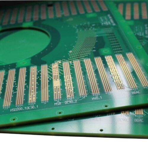
El segundo paso es la fabricación de placas PCB
Los siguientes son los principales procedimientos de producción de tableros multicapa convencionales.
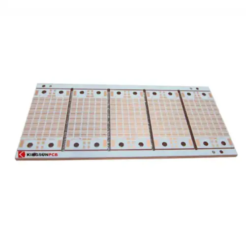
Corte de materiales: El material de corte es el área grande (48 x 42 pulgadas) de materia prima que se corta en el panel de trabajo que necesitan los fabricantes de PCB.
Capa interna: The inner layer of the circuit uses positive imaging technology, After developing, etching, and de-filming processes, complete the production of the inner layer of the line.
Óxido negro: Black Oxide is made before lamination. The main role is to roughen the copper surface and increase the surface contact area with the resin to ensure the quality of lamination.
Laminación: Stack up the inner core and prepreg to press into multilayer board through vacuum pressure machine. And make the tooling holes for the next process.
Drilling: Using CNC drilling machine, through holes are drilled for circuit connections between layers.
Cobre no electrolítico: Electroless copper is chemically deposited, copper. The method deposits a thin copper layer in the non-conductive substrate so that the through-holes are metallization. Then use the plating method to thicken the hole’s copper thickness to achieve the design purpose.
Revestimiento de cobre: El revestimiento de cobre es un método de galvanoplastia para aumentar el espesor de los orificios pasantes y las superficies del circuito.
Capa exterior: Transfiera el patrón exterior a la placa revestida de cobre y grabe el cobre inútil.
Carácter de resistencia a la soldadura: Impresión de una capa de tinta de máscara de soldadura aislada en la superficie de la capa exterior. Algunos PCB también necesitan tener símbolos impresos en la capa de máscara de soldadura.
Surface treatment: Common PCB surface treatments include HASL, OSP, Immersion Gold, ENEPIG, Immersion Silver, Immersion Tin, and Gold finger plating.
Prueba eléctrica: All the PCBs must be pen/short tested before outgoing, the test included electrical test and flying probe test. Electrical test for PCB mass production and flying probe test for samples as it’s fast turn round.