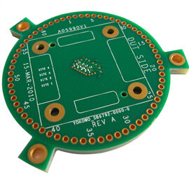
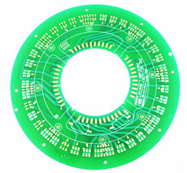
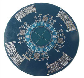
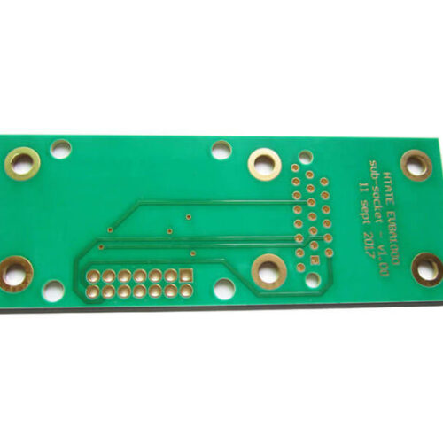
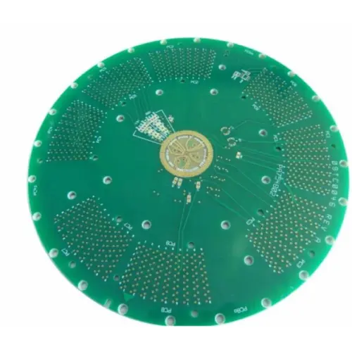
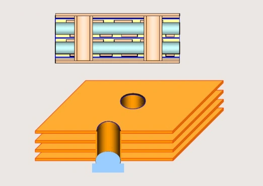
What is HDI PCB?

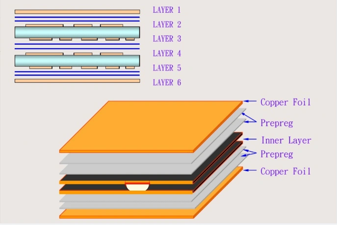
HDI PCB is the abbreviation of high density interconnector PCB. HDI PCB manufacturer makes the HDI board by increased layers through micro-blind&buried vias.

HDI PCB board is a compact product specially designed for small capacity users.

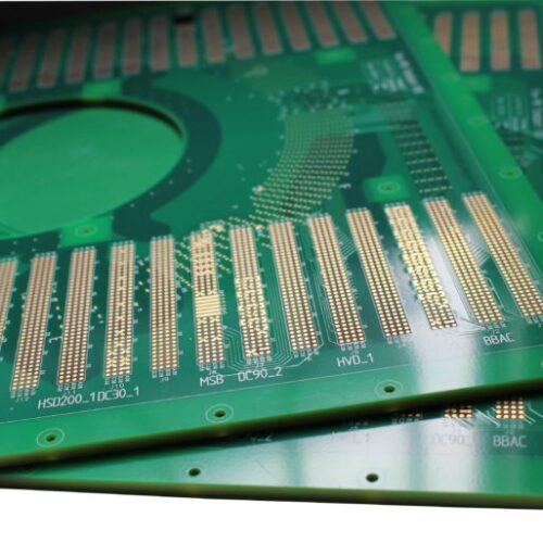
The HDI board includes the following via types:

PCB de microvía: en la industria de PCB, las vías con un diámetro inferior a 150 um (6 mil) se denominan microvías.

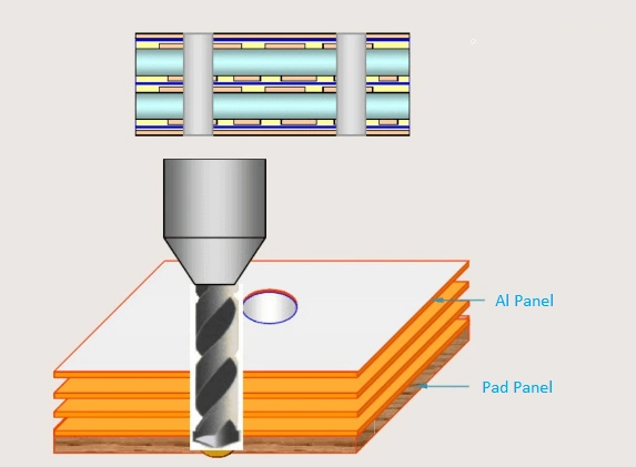
Vías enterradas: Las vías están enterradas en la capa interna, generalmente no visibles en el producto terminado. 

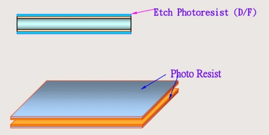
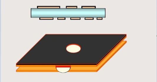
Blind vias: The blind vias are drills from top layer or bottom layer to a certain inner layer. They are not through the whole HDI board. 

Characteristics of HDI PCB Board

Más pequeño y ligero

HDI PCB manufacturer make the HDI PCB board through continuous lamination and laser drilling with a large number of micro-buried blind holes. So it has the advantages of being light, thin, short, and small.

Alta densidad

High density interconnect PCB design with more vias, traces, copper pads and inner layers. The via diameter is usually less than 150um, the line width and line spacing do not exceed 76.2um, also the thickness of the interlayer dielectric is less than 80um.

Mejor rendimiento eléctrico

HDI PCB boards have better electrical performance due to multiple pressing and plating. In addition, the HDI PCB board has better improvement for radio frequency interference, electromagnetic wave interference, electrostatic discharge, heat conduction, etc.

Altos requisitos para vías de conexión

At present, HDI PCB board buried& blind vias plugging technology is painful for HDI PCB manufacturer. Quality problems will involve vias cavity,uneven dielectric thickness and uneven board edge if HDI PCB manufacturer does not do well with buried and blind vias.

Features of HDI PCB Board Manufacturing

The HDI PCB manufacturing process is usually different from that of other standard PCBs, The following are some special characteristics of HDI PCB board manufacturing.

Laminaciones Múltiples

Lamination of PCB core board, PP and copper foil. Unlike other standards PCBs, HDI PCB boards go through the lamination process multiple times. These continuous laminate structures help prevent movement and breakage during drilling.

A través de la tecnología pad

HDI PCB with via in pad technology is that the via be drilled in copper pad and filled with resin or copper materials. Then plating a layer copper to cover the via, so the pad can be used in soldering.

Tipos de vías de llenado

Via filling type should generally be determined based on specific application and PCB requirements. Filling materials used include chemical plating, silver filling, copper filling, conductive resin, and non-conductive resin. The most common via filling material is a non-conductive resin.

Tecnología de perforación láser

Laser drilling is widely used in HDI PCB design. The laser heads can produce laser light up to 20 microns in diameter. It’s easy to cut metal and fiberglass and produce very small and clean vias. Using smooth glass fibers with a lower dielectric constant allows for smaller vias.

Capacidades de fabricación

Artículo Parámetros técnicos    Especificación
Ancho/espacio mínimo de línea del circuito 2,7/2,7 mil Espesor de cobre acabado H oz
Anillo de almohadilla de PCB mínimo de vía  3 millones  Distancia entre el borde del agujero y el borde del anillo 
 Anillo de almohadilla de PCB mínimo de PTH 5 millones  Distancia entre el borde del agujero y el borde del anillo  
 PCB mínimo por tamaño 3 millones  Grosor del tablero < 1,2 mm 
 Grosor mínimo de PCB de 4 capas 0,4 milímetros  Espesor final del tablero
Grosor mínimo de PCB de multicapa 0,4 milímetros Espesor final del tablero
Grosor máximo de PCB  3,2 milímetros  Espesor final del tablero 
 Dimensión máxima de PCB 609×450 milímetros  PCB de una y dos caras
 Espacio entre la línea y el borde del tablero 10 millones  Fresado de contorno 
 Capas máximas de PCB 40 capas   
Color de máscara de soldadura de PCB Verde, Negro, Azul, Rojo, Blanco, Amarillo,  
Color de serigrafía de PCB Blanco, negro, amarillo  
Acabado de superficies de PCB HASL,ENIG,ENEPIG,ImAg,ImTin,OSP, Hard Gold Plating  
Espesor máximo de cobre de acabado 2 onzas  
Espesor dieléctrico 2,5 millones  
Material de PCB FR-4, sustrato de aluminio, Rogers4350C, poliimida  
Tecnología especial Orificio avellanado, vía in Pad PCB, PCB ciego y enterrado  

Tipos de PCB HDI


Acumulación 1+N+1

Sólo existe un taladro ciego y enterrado que conecta directamente dos capas adyacentes. Por ejemplo, la capa 1 y la capa 2 están conectadas o la capa X está conectada a la capa (X-1).

Acumulación 2+N+2

El orificio ciego desde la capa exterior del orificio pasante hasta la tercera capa se puede conectar directamente a la capa 1-3, o se puede conectar a la capa 1-2 y a la capa 2-3 por separado.

cualquier capa

Hay conexiones de microvías entre capas adyacentes. Por ejemplo, L1-L2, L2-L3, L3-L4, L4-L5, L5-L6, L6-L7, L7-L8… etc.

Proceso de fabricación de PCB HDI

Capa interna

The first step is cut material sheet into working panel, then start to make Inner Layer that uses dry film to transfer PCB pattern to the copper clad by exposure and development processes.

King Sun PCB’s inner layer production capability is presently 3mil line/3mil space for Hoz and 1oz copper.

Recubrimiento de óxido negro

Black oxide makes core to have a uniform fluff layer that increases the bond strength between the copper foil and prepregs. It also removes grease and burs from the material surface to ensure cleanliness before lamination.

Laminación de la capa interior

This lamination is made for blind vias and buried vias layers. The first step is stack and fix the prepreg sheet and the oxidized inner layer board in position. Then laminated the copper foils, prepregs and inner layer through automatic pressing machine. 

Some HDI PCBs are multiple laminations for different PCB blind&buried vias designs.

Apilamiento 1+N+1: Este tipo de PCB HDI es de laminación única.

Apilamiento 2+N+2: Este tipo de PCB HDI tiene dos laminaciones.

Stackup Anylayer: This HDI PCB type is multiple laminations.

Perforación de capa interior (vías ciegas y enterradas)

After first lamination, then blind vias and buried vias will be drilled.

When the via diameter is more than 0.2mm, we will use traditional CNC drilling machine.When the via diameter is less than 0.2mml, we will use laser drilling.

Revestimiento de capa interior

After blind vias and buried vias be drilled, the vias need to be plated before outer layer lamination. Board thickness and via diameter aspect ratio is not more than 10 to ensure the via wall plating is good.

Laminación de la capa exterior

The next PCB manufacturing processes are as same as standard multilayer PCB.

La aplicación de PCB HDI

  • Mobile communication devices and notebook computers. Moreholes, light weight, small size, strong function.
  • Computer and network communication equipment and large equipment. Few holes, high layer acounts, impedance control for transmitted signal trace.
  • Portadores de chips para embalaje LSI, incluidos pads y flip chips, etc. Ancho y espaciado de línea pequeños (generalmente menos de 2 mils), alta precisión, apertura pequeña (1-2 mils), espaciado de apertura pequeño (≤5 mils), buen calor Resistencia y pequeño coeficiente de expansión térmica del sustrato.

¿Por qué elegirnos?

Fabricación de PCB de giro rápido

Podemos fabricar prototipos de PCB con un plazo de entrega muy rápido:

Recuento de capas Plazo de entrega estándar Respuesta rápida
1-2 capas 4-5 DÍA 24 horas
4 capas 5-6 DÍA 48 horas
 6 capas 7-8 DÍA 96 horas
 8 capas 9-10 DÍA 140 horas
 10 capas 10-12 DÍA 192 horas
 
Tecnologías de PCB complejas

Fabricamos PCB muy complejos y especiales como los siguientes:

  • Vía en Pad PCB
  • PCB de moneda de cobre integrado
  • PCB de retroperforación
  • PCB con ranura de profundidad
  • PCB con orificio avellanado
  • Vías ciegas y enterradas PCB