Rigid PCB-How are PCB circuit boards tested-KingSunPCB

What is Rigid PCB?

Rigid PCB board is a conventional Printed Circuit Board. It cannot be bent or flexed.

A Rigid PCB board is one of the important components of electronics product manufacture. Almost every electronic product must be used PCB board, from small watches, and calculators to computers, electronic communication equipment, and even military weapon systems.

Types of Rigid PCB Board

Single Layer Rigid PCB

Single layer rigid PCB is the most basic PCB. Components are concentrated on one side and circuits are concentrated on the other side. Single layer PCB board has many strict restrictions on the design circuit (because there is only one side, the wiring can not cross and must go around the unique path), only the early circuits use this kind of board.

2-Layer Rigid PCB

2-Layer Rigid PCB Board circuits on both sides of this board, to use both circuits, proper circuit connections must be made between the two sides. This “bridge” between circuits is called a via. The via hole is on the PCB board, filled with or coated with a metal hole, and it can be connected to the wires on both sides. Because the area of the dual panel is double that of the single panel, the dual panel solves the difficulty of wiring in a single panel (via conduction through the hole to the other side), which is more suitable for use in more complex circuits than a single panel.

Multilayer Rigid PCB

4 Layer rigid PCB, 6 Layer rigid PCB, 8 Layer rigid PCB and more layers, we call them mulitlayer rigid PCB.

In order to increase the area that can be routed, multilayer rigid PCB boards use more single or double-sided wiring boards.

Usually, the number of layers is even, and the outermost two layers are included. Most of the motherboards are 4 layer to 8 layer structures.

Super-multi-layer boards have gradually become unused. Because the layers in the PCB are tightly integrated, it is generally not easy to see the actual number, but if you look closely at the motherboard, you can still see it.

Merkmale der starren Leiterplatte

Starre Leiterplatten können immer breiter eingesetzt werden, da sie über viele einzigartige Vorteile verfügen, die im Folgenden beschrieben werden.

Density Can Be Increased of Rigid PCB

For decades, the high density of rigid PCBs has grown as integrated circuits have become more integrated and installation technologies have advanced.

Hohe Zuverlässigkeit

Through a series of inspections, tests, and aging tests, the rigid PCB circuit board can be reliably operated for a long period of time (usually 20 years).

Designability

For rigid PCB performance (electrical, physical, chemical, mechanical, etc.) requirements, PCB circuit board design can be achieved through design standardization, standardization, etc., with short time and high efficiency.

Productivity of Rigid PCB

With modern management, we can carry out standardization, scale (quantity), automation and other production, and ensure the consistency of product quality.

Rigid PCB Testability

Established a relatively complete test method, test standards, a variety of test equipment and instruments to detect and identify the qualification and service life of rigid PCB circuit board products.

Rigid PCB Assemblability

Rigid PCB board products not only facilitate the standard assembly of various components, but also can be automated, large-scale mass production. At the same time, PCB circuit board and various component assembly parts can also be assembled to form larger parts and systems up to the complete machine.

Wartbarkeit

Since rigid PCB products and various component assembly parts are produced with standardized design and scale, these components are also standardized. Therefore, once the system fails, it can be quickly, easily, and flexibly replaced, quickly recovering from the system’s work. Of course, you can also give more examples. For example, the system is miniaturized, lightweight, and the signal transmission speed is increased.

Starres PCB-Material

The main raw materials commonly used in rigid PCB are substrate, copper foil, PP, photosensitive material, solder mask and film.

Rigid PCB Substrate

Copper-clad laminate is a composite material made from wood pulp paper or glass fiber cloth as a reinforcing material that is impregnated with resin and then covered on one or both sides with copper foil. It undergoes a hot-pressing process. In the production of rigid PCB multilayer boards, this material is commonly referred to as the core board or CORE.

Rigid PCB Copper Foil

The copper foil serves as the cathode component of the electrolytic material, and is deposited onto a thin continuous metal layer on the rigid PCB substrate

Äußerlich kann es leicht mit der Isolierschicht verbunden werden, die die Schutzschicht aufnimmt und geätzt wird, um Ihr Schaltungsmuster zu erstellen.

Die Dicke von starrem PCB-Kupfer wird typischerweise in die Varianten 1oz (35µm), 2oz (70µm) und 3oz (105µm) eingeteilt.

Rigid PCB Prepreg

PP is a thin insulation material used for rigid printed circuit boards. Prior to being laminated, PP is in the form of a prepreg, also known as pre-impregnated fiber. It is primarily utilized as the adhesive and insulating material for the inner conductive pattern of multilayer circuit boards.

Once the PP has been laminated, the semi-cured epoxy is forced out, begins to flow, and ultimately solidifies, creating a strong bond that joins the multilayer circuit boards together, resulting in a dependable insulating layer.

Lichtempfindliches Material

These materials are generally classified as either photoresist or photosensitive film, and within the industry they are further divided into wet and dry film categories

When exposed to certain wavelengths of light, wet-film coatings on rigid PCB copper clad laminates undergo a chemical transformation that alters their solubility in the developer (solvent).

Dry film is further categorized into positive and negative film, differentiated by their photodegradable and photopolymerizable properties. Both types are highly sensitive to ultraviolet rays

Lötstopplackfolie

This is a typical liquid photosensitive material that has no compatibility with liquid solder. It undergoes a chemical transformation and solidifies under specific lighting conditions. There are various ink colors available, with green being the most frequently used color for solder mask.

Möglichkeiten zur Herstellung starrer Leiterplatten

Artikel Technische Parameter    Spezifikation
Min. Breite/Abstand der Stromkreisleitung 3/2,7 Mio. Fertige Kupferstärke H oz
Minimaler starrer PCB-Pad-Ring oder Via  3 Mio  Abstand zwischen Lochrand und Ringrand 
 Minimal starrer PCB-Pad-Ring aus PTH 5 Mio  Abstand zwischen Lochrand und Ringrand  
 Mindestgröße für starre Leiterplattendurchkontaktierungen 4 Mio  Plattenstärke < 1,2 mm 
 Mindestdicke der starren doppelseitigen Leiterplatte 0,2 mm  Endgültige Plattendicke
Mindestdicke der starren Mehrschicht-Leiterplatte 0,4 mm Endgültige Plattendicke
Maximale Dicke starrer Leiterplatten  8.0 mm  Endgültige Plattendicke 
 Maximale Abmessung starrer Leiterplatte 609×609 mm  Ein- und doppelseitige Leiterplatte
 Abstand zwischen Linie und Brettkante 10 Mio  Konturfräsen 
 Maximale Anzahl starrer PCB-Lagen 30 Schicht   
Farbe der Lötstoppmaske für starre Leiterplatten Grün, Schwarz, Blau, Rot, Weiß, Gelb,  
Siebdruckfarbe für starre Leiterplatten Weiß, Schwarz, Gelb  
Oberflächenbearbeitung starrer Leiterplatten HASL, ENIG, ENEPIG, ImAg, ImTin, OSP, Hartvergoldung  
Maximale Endkupferdicke 6 Unzen  
Dielektrikumsdicke 2,5 Mio  
Starres PCB-Material FR-4, Aluminiumsubstrat, Rogers4350C, Polyimid  
Spezielle Technologie HDI-Leiterplatte, Via-in-Pad-Leiterplatte, Blind- und vergrabene Leiterplatte  

Möglichkeiten zur Herstellung starrer Leiterplatten

Below is the basic production process of China Rigid PCB factory.

CNC-Bohren

In order to increase rigid PCB assembly density, the vias on the double-sided circuit board of the PCB circuit board are getting smaller and smaller. Generally, double-sided PCB circuit boards are drilled with CNC tolling machines to ensure accuracy.

Rigid PCB Plating Hole Process

Plating hole process, also known as metallized hole, it’s a process of electroplating the entire hole wall with metal, so that the conductive pattern between the inner and outer layers of the double-sided rigid printed circuit board can be electrically interconnected.

Lötstopplack und Siebdruck

Der Siebdruck wird für den Lötstopplackdruck und den Symboldruck verwendet.

Rigid PCB Surface Finish

Hot Air Solder Leveler(HASL), ENIG, and OSP are the most common surface finish of rigid PCB circuit board because of their good electrical

Rigid PCB Milling

The rigid PCB board has been cycling in the final process of milling, CNC machine follows the PCB board outline gerber to route the PCB circuit outline.

Mahlen

Stromkreisunterbrechung/Kurzschlusstest

Der letzte Schritt bei der Herstellung starrer Leiterplatten ist ein Unterbrechungs-/Kurzschlusstest, um die Qualität der starren Leiterplatte sicherzustellen.

Allgemeine Muster und kleine Chargen von starren Leiterplatten werden mit fliegenden Sonden getestet, was die Kosten für die Herstellung von Testrahmen senken und den Lieferzyklus verkürzen kann. Die in Massenproduktion hergestellten starren Leiterplatten werden mit Testwerkzeugen getestet.

Vakuumverpackung

Good rigid PCBs boards are vacuum packaged and prepare for shipment.

Möglichkeiten zur Herstellung starrer Leiterplatten

Below is the basic production process of China Rigid PCB factory.

Eingehende Qualitätskontrolle

Following Standard inspection procedure to do material incoming inspection, like copper clad laminate, solder mask oil, etc.

Qualitätskontrolle im Prozess

Process control is a very important part of rigid PCB fabrication.KingSun follows standard production processes and strictly controls each process. Especially for key links, detailed records and monitoring should be carried out in order to solve problems in the production process.

Abschließende Qualitätskontrolle

After the production is completed, it needs to go through a series of inspection and acceptance links, which is also an important measure to ensure high quality rigid PCB.

Ausgangsqualitätskontrolle

Before the product is shipped, an inspection is carried out to ensure that the shipped product meets the customer’s quality requirements. Only products that pass the inspection can be shipped.

Anwendung von starren Leiterplatten

Anwendung von starren Leiterplatten

Rigid And Flex PCB Materials Are Different

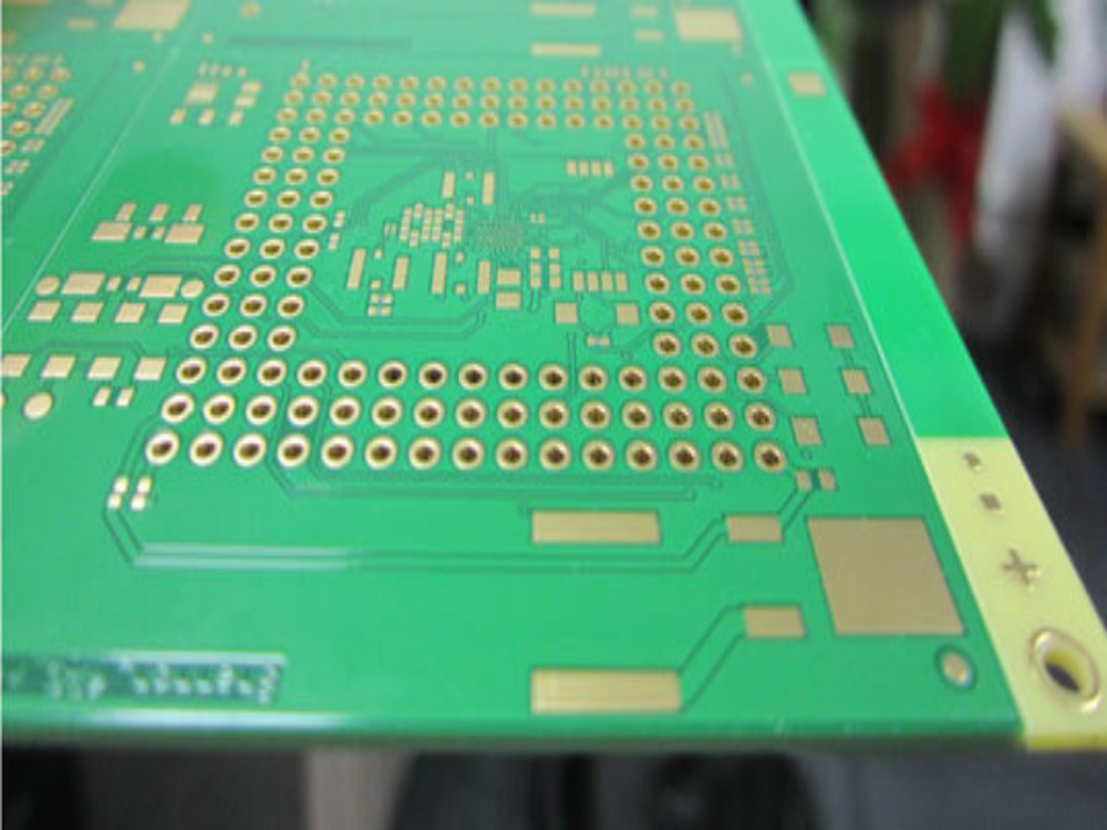
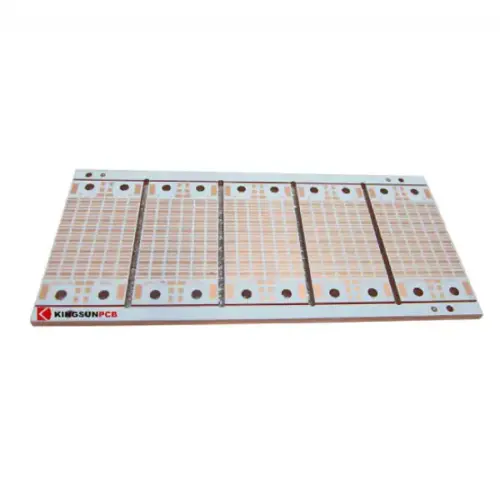
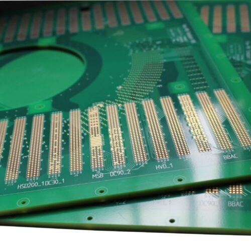
Rigid PCB board is a circuit board made of hard materials such as glass fiber reinforced resin.

Rigid PCB materials include phenolic paper laminate, epoxy paper laminate, polyester glass felt laminate and epoxy glass cloth laminate.

Flex PCB board is a flexible circuit board made of polyimide and polyester material, etc. The typical feature of the flexible board is the insulating film, and the flexible board uses a thin and soft insulating film to achieve insulation and mechanical strength.

Rigid And Flex PCB Design Are Different

Rigid PCB design is to realize the integration of the circuit by laying out the electronic components on the circuit board, thereby improving the performance of the circuit, reducing failure and maintenance costs.

Flexible PCB circuit boards are designed to meet the needs of specific application scenarios, such as space-limited electronic devices that need to be bent, folded, or bent.

Rigid And Flex PCB Applications Are Different

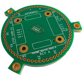
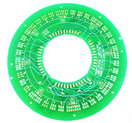
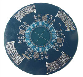
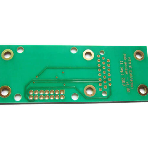
Rigid PCB is often used in applications that need to be stronger, such as inside computers or in some mechanical and industrial products.

The electrical performance of the rigid PCB board is more stable and reliable, and it is not easy to be deformed or damaged. They will not affect their performance due to changes in the environment and can be more suitable for high-density wiring.

Flexible Leiterplatten werden häufig in Anwendungen eingesetzt, die Biegen und Krümmen erfordern, wie beispielsweise bei einigen hochpräzisen, leichten elektronischen Geräten, Uhren, Autokarosserien usw.

Advantages Of Rigid And Flex PCB

Rigid PCB board has the characteristics of firmness, wear resistance, high temperature resistance, etc., and has good thermal performance, which can evenly distribute the heat generation of components.

multilayer rigid PCB can connect multiple circuits together, effectively reducing space and making the originally complicated circuits more compact.

FPC PCB board has higher flexibility, adaptability and can assemble electronic components in more complex shapes.

In addition, FPC circuit board also has the advantages of being lightweight, small size and high reliability, so it is widely used in mobile devices, wireless communications, medical equipment, automotive electronics and other fields.

Warum uns wählen?

Schnelle Fertigung starrer Leiterplatten

We can make quick turn FR4 rigid PCB prototype with a very fast turnaround lead time.

PCB prototypes can be quickly produced for PCB board circuit testing and verification in the early stage of product development, improving the efficiency of product development, thereby shortening the project cycle. Below is the quick turn rigid PCB lead time:

Anzahl der Schichten Standardlieferzeit Schnell umdrehen
1-2-lagige Leiterplatte 4-5 TAGE 24 Stunden
4-Schicht-Leiterplatte 5-6 TAGE 48 Stunden
 6-lagige Leiterplatte 7-8 TAGE 96 Stunden
 8-lagige Leiterplatte 9-10 TAGE 140 Stunden
 10-Schicht-Leiterplatte 10-12 TAGE 192 Stunden

Komplexe starre Leiterplattentechnologien

Wir fertigen sehr komplexe und spezielle starre Leiterplattenschaltungen wie die folgenden:

  • Via in Pad starre Leiterplatte
  • Eingebettete starre Kupfermünzen-Leiterplatte
  • Rückbohren von starren Leiterplatten
  • Tiefe Schlitz starre Leiterplatte
  • Senkloch für starre Leiterplatte
  • Blinde und vergrabene Durchkontaktierungen für starre Leiterplatten