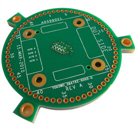
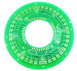
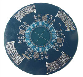
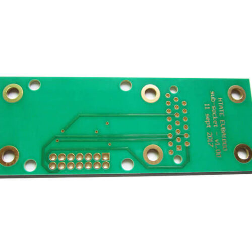
Features of HDI PCB Board Manufacturing
The HDI PCB manufacturing process is usually different from that of other standard PCBs, The following are some special characteristics of HDI PCB board manufacturing.
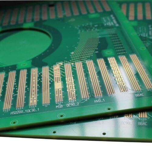
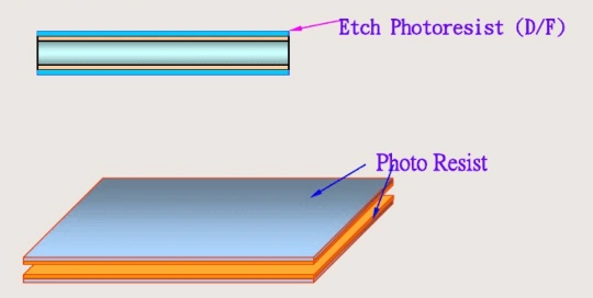
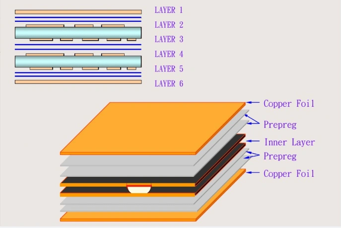
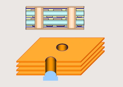
Multiple Laminations
Lamination of PCB core board, PP and copper foil. Unlike other standards PCBs, HDI PCB boards go through the lamination process multiple times. These continuous laminate structures help prevent movement and breakage during drilling.
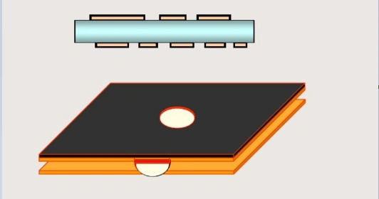
Via in pad Technology
HDI PCB with via in pad technology is that the via be drilled in copper pad and filled with resin or copper materials. Then plating a layer copper to cover the via, so the pad can be used in soldering.
Filling vias Types
Via filling type should generally be determined based on specific application and PCB requirements. Filling materials used include chemical plating, silver filling, copper filling, conductive resin, and non-conductive resin. The most common via filling material is a non-conductive resin.
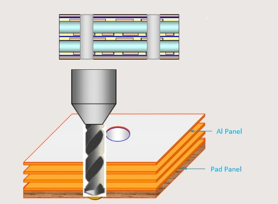
Laser Drilling Technology
Laser drilling is widely used in HDI PCB design. The laser heads can produce laser light up to 20 microns in diameter. It’s easy to cut metal and fiberglass and produce very small and clean vias. Using smooth glass fibers with a lower dielectric constant allows for smaller vias.