O que é fabricação de PCBA?

PCBA is the abbreviation of Printed Circuit Board Assembly. PCBA manufacturing is the process of attaching electronic components to a Printed Circuit Board by SMT production and through hole assembly. This process involves a combination of automated and manual tasks such as soldering, surface mount technology (SMT), through-hole technology (THT), and quality inspection. PCBA manufacturing is an essential step in electronic devices.

Teste de Circuito Aberto/Curto

The last step of rigid PCB manufacture is open/short circuit test to ensure the quality of the rigid PCB board.

General samples and small batches of rigid PCB circuit boards are tested with flying probes, which can reduce the cost of making test frames, then shorten the delivery cycle. The mass-production rigid PCB boards are tested by test tooling.

A fabricação do PCBA começa no design do PCB

Preparação preliminar do projeto de PCB

PCB board size and layer count need to be determined in the early stages of PCB design. The layer count will directly affect the PCB routing and impedance. The PCB dimension will help to achieve the purpose of PCB design.

Projeto de layout de PCB

In the PCB design process, the first is the correct layout, which is the most basic PCB design entry requirement. Secondly, the electrical performance, which is a measure of a PCB board is a qualified standard.Once again, optimize the PCB circuit routing to meet test convenience, neat and tidy.

Inspeção na RDC

Quality control is an important part of PCB design. It includes Self-inspection, mutual inspection, special inspection, etc. Check whether the empty foot of each component is normal and whether it is a leakage line. Check whether the upper and lower wiring of the same network table has holes, and whether the pads are connected through the holes to prevent wire breakage and ensure the integrity of the line.

A segunda etapa é a fabricação de placas PCB

A seguir estão os principais procedimentos de produção de placas multicamadas convencionais.

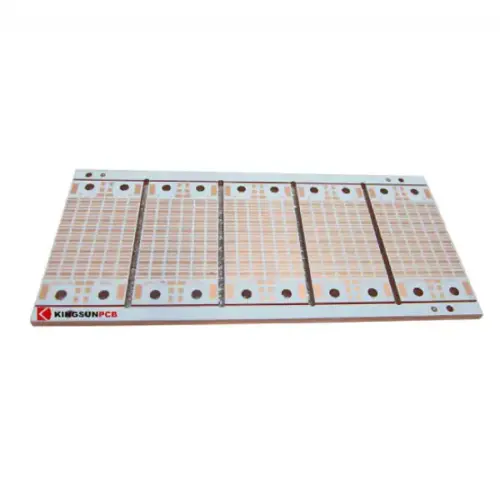
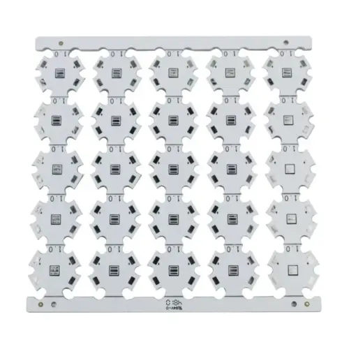
Corte de materiais: O material de corte é a grande área (48 pol. * 42 pol.) De matéria-prima que é cortada na placa do painel de trabalho necessária aos fabricantes de PCB.

Camada interna: The inner layer of the circuit uses positive imaging technology, After developing, etching, and de-filming processes, complete the production of the inner layer of the line.

Óxido Preto: Black Oxide is made before lamination. The main role is to roughen the copper surface and increase the surface contact area with the resin to ensure the quality of lamination.

Laminação: Stack up the inner core and prepreg to press into multilayer board through vacuum pressure machine. And make the tooling holes for the next process.

Drilling: Using CNC drilling machine, through holes are drilled for circuit connections between layers.

Cobre eletrolítico: Electroless copper is chemically deposited, copper. The method deposits a thin copper layer in the non-conductive substrate so that the through-holes are metallization. Then use the plating method to thicken the hole’s copper thickness to achieve the design purpose.

Chapeamento de cobre: O revestimento de cobre é um método de galvanoplastia para aumentar a espessura dos orifícios passantes e das superfícies do circuito.

Camada externa: Transfira o padrão externo para a placa revestida de cobre e grave o cobre inútil.

Caráter de resistência à solda: Imprimindo uma camada de tinta de máscara de solda isolada na superfície da camada externa. Alguns PCBs também precisam ter símbolos impressos na camada da máscara de solda.

Surface treatment: Common PCB surface treatments include HASL, OSP, Immersion Gold, ENEPIG, Immersion Silver, Immersion Tin, and Gold finger plating.

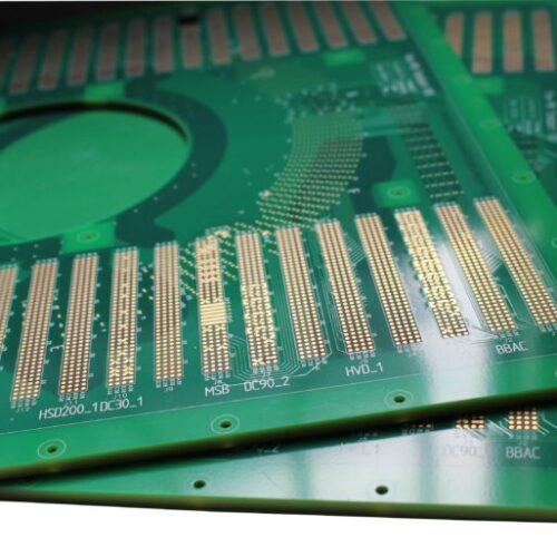
Teste Elétrico: All the PCBs must be pen/short tested before outgoing, the test included electrical test and flying probe test. Electrical test for PCB mass production and flying probe test for samples as it’s fast turn round.

Tipos de fabricação de PCBA

Existem dois tipos principais de fabricação de PCBA: Tecnologia de Montagem em Superfície (SMT) e Tecnologia Através de Furo (THT).

Tecnologia de montagem em superfície (SMT)

A montagem SMT da placa de circuito impresso é uma tecnologia de montagem de circuito que solda componentes na superfície de uma placa de circuito impresso por soldagem por refluxo ou soldagem por imersão. A fabricação de SMT PCBA é normalmente usada para dispositivos eletrônicos compactos, leves e de alta densidade, como smartphones, tablets e laptops.

Tecnologia de furo passante (THT)

Through-hole Printed Circuit Board assembly also named DIP involves inserting electronic components through pre-drilled holes in the PCB, and then soldering the leads to the other side of the board. Through-hole Printed Circuit Board assembly is used for heavy-duty electronic devices, such as industrial equipment and high-end audio gear.Most electronic devices are the combination of both SMT and THT assembly methods to achieve a balance between size, weight, and durability.

Características de fabricação de PCBA

Here are some characteristics of PCBA manufacturing

Montagem de Densidade

O conjunto da placa de circuito impresso pode ser um produto eletrônico de alta densidade, leve e de pequeno volume. Geralmente, o volume de produtos eletrônicos é reduzido em 40%-60% e o peso é reduzido em 60%-80% após usar o processo SMT.

Alta fiabilidade

PCBA manufacturing is high reliability, strong vibration resistance, and low solder joint defect rate.

Anti-Interferência

PCBA manufacturing has the strong anti-interference ability and better electromagnetic compatibility.

Automação

A maior parte da fabricação de PCBA é automatizada usando máquinas especializadas. Isto não só aumenta a eficiência da produção, mas também garante consistência e precisão, além de reduzir custos de materiais e tempo de mão de obra.

Materiais de fabricação de PCBA

PCBA manufacturing mainly uses three major materials, which are solder paste, flux, and SMT glue.

Pasta de solda

Solder paste is made of alloy solder powder and paste flux evenly stirred, it is an indispensable soldering material in the SMT chip processing process, widely used in reflow soldering. Solder paste has a certain viscosity at room temperature, and can be electronic components initially stick in the established position. 

Fluxo

Flux is the carrier of tin powder, and its composition is basically the same as that of general-purpose flux. In order to improve the printing effect, it is sometimes necessary to add an appropriate amount of solvent, through the action of the activator in the flux.

Cola SMT

A cola SMT, também conhecida como adesivo SMT, ou cola vermelha SMT, é geralmente uma pasta vermelha (também amarela ou branca) que é distribuída uniformemente com endurecedores, pigmentos, solventes, etc., usada principalmente para fixar os componentes na placa impressa. Geralmente, usamos o método de distribuição ou impressão em estêncil para distribuir e, em seguida, colocamos os componentes no forno ou forno de refluxo para aquecer e endurecer.

PCB Manufacturing Fabrication Capabilities

Item Parâmetros técnicos    Especificação
Largura/espaço mínimo da linha do circuito 3/2,7 mil Espessura de cobre acabada H oz
Anel mínimo de almofada PCB da Via  3 milhões  Distância entre a borda do furo e a periferia do anel 
 Anel mínimo de almofada PCB de PTH 5 milhões  Distância entre a borda do furo e a periferia do anel  
 PCB mínimo por tamanho 4 milhões  Espessura da placa < 1,2 mm 
 Espessura mínima do PCB de dupla face 0,2 mm  Espessura Final da Placa
Espessura mínima do PCB de multicamadas 0,4 mm Espessura Final da Placa
Espessura máxima do PCB  8,0mm  Espessura Final da Placa 
 Dimensão máxima do PCB 609×609 milímetros  PCB de face única e dupla
 Espaço entre a linha e a borda da placa 10 milhões  Fresagem de Contorno 
 Máximo de camadas de PCB 30 camadas   
Cor da máscara de solda PCB Verde, preto, azul, vermelho, branco, amarelo,  
Cor da serigrafia PCB Branco, preto, amarelo  
Acabamento de superfície PCB HASL,ENIG,ENEPIG,ImAg,ImTin,OSP, chapeamento de ouro duro  
Espessura máxima de cobre de acabamento 6 onças  
Espessura dielétrica 2,5 milhões  
Material PCB FR-4, substrato de alumínio, Rogers4350C, poliimida  
Tecnologia Especial HDI PCB, via in Pad PCB, PCB cego e enterrado  

Como fazer a fabricação de PCBA?

Item Parâmetros técnicos    Especificação
Largura/espaço mínimo da linha do circuito 3/2,7 mil Espessura de cobre acabada H oz
Anel de almofada PCB rígido mínimo da Via  3 milhões  Distância entre a borda do furo e a periferia do anel 
 Anel de almofada de PCB rígido mínimo de PTH 5 milhões  Distância entre a borda do furo e a periferia do anel  
 PCB rígido mínimo por tamanho 4 milhões  Espessura da placa < 1,2 mm 
 Espessura mínima de PCB rígida de dupla face 0,2 mm  Espessura Final da Placa
Espessura mínima de PCB rígida de multicamadas 0,4 mm Espessura Final da Placa
Espessura máxima de PCB rígida  8,0mm  Espessura Final da Placa 
 Dimensão máxima do PCB rígido 609×609 milímetros  PCB de face única e dupla
 Espaço entre a linha e a borda da placa 10 milhões  Fresagem de Contorno 
 Camadas rígidas máximas de PCB 30 camadas   
Cor rígida da máscara de solda PCB Verde, preto, azul, vermelho, branco, amarelo,  
Cor rígida da serigrafia PCB Branco, preto, amarelo  
Acabamento de superfície de PCB rígido HASL,ENIG,ENEPIG,ImAg,ImTin,OSP, chapeamento de ouro duro  
Espessura máxima de cobre de acabamento 6 onças  
Espessura dielétrica 2,5 milhões  
Material rígido de PCB FR-4, substrato de alumínio, Rogers4350C, poliimida  
Tecnologia Especial HDI PCB, via in Pad PCB, PCB cego e enterrado  

Como fazer a fabricação de PCBA?

Impressão em pasta de solda

Accurately apply solder paste or adhesive onto the PCB pads in preparation for component placement.There are three types solder paste machines: manual printing machines, semi-automatic printing machines and fully automatic printing machines.


Montar

Utilize the equipment-edited program to precisely position the components onto the designated locations of the PCB.The placement machine involves high-speed placement machine and multi-function placement machine.High-speed placement machines are generally used to mount small chip components.The multi-function placement machine is mainly used to mount roll-shaped, disc-shaped or tubular large components or abnormal shape components.

Refluxo

Posicionado atrás da máquina de colocação na linha de produção SMT, este dispositivo cria um ambiente aquecido que facilita o derretimento da pasta de solda na almofada. Como resultado, os componentes de montagem em superfície e as placas de PCB são firmemente unidos usando pasta de solda.

AOI

When AOI is automatically detected, the machine scans the PCB through its camera, automatically collecting images. It then compares the tested solder joints with qualified parameters stored in the database, and checks for defects on the PCB through image processing. Any defects are displayed and marked on the display, allowing maintenance personnel to quickly identify and repair them.

A aplicação da fabricação de PCBA

PCBA manufacturing is an important technology that enables the development of complex electronic devices that are used in a wide range of industries and applications. Below are some common applications.

Consumer electronics

PCBA manufacturing is used in a range of consumer electronics, including smartphones, tablets, laptops, televisions, and home appliances.

Automotivo

PCBA manufacturing is used in automotive applications for electronic control units, sensors, and other critical components.

Industrial automation

PCBA manufacturing is used in industrial automation applications for controlling machinery, monitoring sensors, and handling data.

Medical equipment

PCBA manufacturing is used in medical equipment for patient monitoring, diagnostics, and treatment.

Aerospace and defense

PCBA manufacturing is used in aerospace and defense applications for controlling and monitoring aircraft systems, satellite communication, and military equipment.

Porque escolher-nos?

PCBA manufacturing in King Sun can offer a combination of affordability, quality, and scalability that makes it an attractive option for businesses. There are several advantages of PCBA manufacturing in King Sun.

Baixo custo

PCBA manufacturing in King Sun is typically much more cost-effective than in many other factories, due to the lower cost of labor and materials.

Alta qualidade

Despite the lower cost, PCBA manufacturing in King Sun can still be of high quality. We imported production and testing equipment from the United States, Japan, and other countries to help companies improve PCBA manufacturing and testing capabilities.

Produção em larga escala

King Sun is one of the largest producers of Printed Circuit boards and PCBA in China, which means that it has the capacity to produce large quantities of circuit boards and PCBA manufacturing quickly and efficiently.

Escalabilidade

King Sun has experience in producing circuit boards for a wide range of applications and industries, including automotive, telecommunications, and consumer electronics. This means that we can scale our production to meet the needs of different clients.

Retorno Rápido

King Sun has our own Printed Circuit Board factory and assembly factory, so the lead times can be very fast than other suppliers, which can be a significant advantage for clients who need their products quickly.