Comprendre les vias PCB, les éléments essentiels pour connecter les couches au sein d'un PCB, est crucial pour une conception haute performance.
Ce guide aborde des notions de base telles que les tailles de tampons et de forets et les capacités du fabricant. Nous explorerons via des stratégies de placement pour minimiser l'inductance, améliorer l'assemblage et éviter les vides. Nous couvrirons également la couture des vias PCB à des fins de blindage.
Qu'est-ce qu'un Via ?
We all know traces are connections on a plane. So, on a layer, we can route anywhere on that plane, usually called a trace. Or we can use things such as copper pours.
However, we must use a via once we want to route between layers, such as connecting layer one to layer three.
Essentially, it’s just a vertical connection in the third dimension. It is used for connections between layers, so our trace on one layer can jump to any or multiple layers in a PCB. We don’t just have to end up on one layer.
If we’re not connecting to a specific layer via a link, we will create a void on that layer, and we’ll look at that in more detail later.
Types de vias
Les cartes de circuits imprimés sont empilées avec des couches de circuits en feuille de cuivre, avec des vias se connectant entre les différentes couches de circuits. Le coût du forage peut aller jusqu'à 30%-40% de la carte entière.
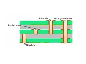
Le trou traversant plaqué (PTH), le trou borgne (BVH) et le trou enterré (BVH) sont les types standard dans les vias de conception de PCB. Les détails de ces trois types de substrats via des trous sont présentés ci-dessous.
Trou traversant plaqué (PTH)
Plated through-holes are the most common PCB vias. If you face the board to the light and see the light, it’s a “through hole.” Incorporating a laser will significantly assist you in making a complete borehole.
Furthermore, the cost will be relatively low. However, in some cases, no through holes are required. It’s cheaper, but it may need more board space.
There are usually two types of through holes: PTH and NPTH. The difference between the two is whether it has copper or not.
PTH holes do not have copper and are often used for inserting electronic components (the hole diameter is slightly larger). It is also used to connect patterns on the inner and outer layers.
Salle de bière aveugle (BVH)
Unlike through-hole vias that pass entirely through the PCB, blind vias connect the outermost layer and a single, specific inner layer.
Since the via doesn’t emerge on the opposite side of the board, it’s called a “blind path.” This technique allows for more efficient use of space on the PCB’s surface.
This manufacturing method requires attention to the hole depth (Z-axis). Because hole plating is complex, only some board manufacturers use this method.
Enterré via trou (BVH)
A buried via hole is a hole that connects to any circuit layer on the board without passing through the outer layer.
This process cannot be carried out using the method of drilling and bonding but requires the drilling process to be made into individual circuit layers, followed by plating and then lamination pressing, which are repeated in three steps.
It takes longer to manufacture than “through hole” and “blind via hole,” and its price is the highest.
HDI PCBs often incorporate blind vias to maximize space for additional circuit layers. Besides drill sizes, pad sizes, and annular rings, many other parameters make up a via.
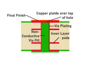
For example, PCB via tenting, which covers the via with the solder mask, typically costs no extra; filling the via will be additional.
Quelles sont les différences entre les différents types de vias ?
One can be sure through-hole vias were made with a drill. Different drill sizes are used, but generally, nothing less than 0.2 mm is used. They go up from there to very much bigger ones.
The drills make the holes under digital control using numerically controlled machines.
As a general rule, multi-spindle tools are used. Subsequently, the tiny holes are made in batches, one after the other. It takes a finite time, and linear motors control the spindles. They turn relatively fast to achieve a good hole quality.
Fonctionnalité des vias
Lorsque nous parlons de vias, nous avons des paramètres principaux spécifiques. Les vias PCB sont essentiels pour accélérer des fonctions complexes sur un PCB en couches. Explorons chacun :
Routage des signaux :
Without through-hole vias, signals could not travel from one layer of the PCB to another. Vias’ role is similar to that of electrical lifts, as they help provide interconnection between different layers. Therefore, this allows the designers to have complex networks and ensure fast signals are effectively transmitted.
Distribution d'énergie et de terre :
Les vias sont cruciaux pour fournir l'alimentation et la terre dans tout le PCB. Ils connectent l’alimentation et les plans de masse sur différentes couches. Par la suite, ils assurent une alimentation en tension stable et constante à tous les composants. De plus, les vias PCB minimisent les chutes de tension et maintiennent l'intégrité du signal.
Routage d'évacuation :
La technologie de montage en surface (SMT) a des pistes. Ces pistes doivent se connecter aux couches internes. Les vias, en particulier les vias traversants, fournissent une voie d'évacuation pour ces connexions.
Quelles sont les règles de routage d'un PCB ?
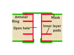
C'est très important. Parlons des règles de routage pour les trous traversants. Selon les normes IPC, un trou doit être centré sur le patin. Selon l'IPC et l'ISO, un trou tangentiel au plot est autorisé, mais le matériau du circuit imprimé peut bouger et les machines ont une tolérance. Pour ces raisons, le tampon doit être plus grand que le diamètre du trou.
If you take the example of a pad of 0.55 mm, you can drill a hole of 0.3 mm. This will give us a finished hole between 0.2 and 0.25 mm, which is relatively small. Similarly, in this case, we must allow isolation on the internal layers of the order of 750 µ if we don’t want a connection.
Aussi, extérieurement, il nous faut une ouverture centrale dans le vernis d'environ 450 µ. C'est environ 1/2 de plus que le diamètre percé. Concernant les micro vias laser, au niveau conception PCB, la norme est d'avoir un plot de 300 µ. Ici, le trou fini sera d'environ 100 µ. Dans ce cas, on peut aller un peu plus serré jusqu'à un minimum de 275. Rappelons donc que les vias laser sont décalés des plots du BGA.
Comment choisir le via dans la conception de mon PCB ?
It isn’t easy to give general via diameters and parameters you should always use. It depends on the scenario you’ll need. If you’re routing out a very fine-pitch BGA, your via needs will be completely different from routing out an audio through-hole board.
Nous devons cependant prendre en compte certaines choses. Une petite taille de foret, par exemple, quelque chose comme 0,15 millimètres ou moins de 0,2 millimètres, entraînera généralement une augmentation du coût des PCB et un rendement inférieur.
Via les paramètres
This term refers to the size and conduct of the hole. It consists of pad size (overall diameter of the hole), drill size (the actual size of the hole), and annular ring (hole’s space from a pad).
Their manufacturer capabilities determine the least drill size and ring width they can produce reliably.
Par placement :
Where you position your vias is essential! Proper choice will reduce inductance (electrical resistance), which can affect signal integrity at high frequencies.
It also guarantees components that can be adequately soldered in assembly and adds to it.
It also helps avoid “voids”- these refer to unoccupied areas on a substrate that might weaken it.
Types d'intermédiaires
There is not just one kind of via! Through-hole vias are prevalent types crossing the entire board.
Blind vias only connect inner layers with themselves without going up to the surfaces of PCBs.
On the other hand, Buried vias do not go through to any external layers but are located between internal layers only. Microvias are small holes found on high-density printed circuit boards (PCBs).
The decision regarding via type entirely depends on PCB design requirements.
Via le dimensionnement
Via sizing involves trade-offs. Smaller vias may save space but increase manufacturing costs and yield higher inductance values; Larger ones take more space but are more accessible for manufacturers.
These general recommendations provide some guidance. However, the best size depends on what you want your application for.
Again, it depends entirely on the scenario. But I often get asked this question: “What via size do you recommend?” And as a general starting point, this seems about right.
When talking about vias, we also need to think, as with traces, about the current handling capabilities.
Conclusion
In conclusion, vias are decisive in the building blocks of any complex printed circuit board.
We have tried to provide various types, parameters, and placement strategies for designing high-performance electronics.
Learning about vias helps create complex connections and bring your PCB designs to life.