Qu'est-ce que la fabrication de PCBA ?

PCBA is the abbreviation of Printed Circuit Board Assembly. PCBA manufacturing is the process of attaching electronic components to a Printed Circuit Board by SMT production and through hole assembly. This process involves a combination of automated and manual tasks such as soldering, surface mount technology (SMT), through-hole technology (THT), and quality inspection. PCBA manufacturing is an essential step in electronic devices.

Test circuit ouvert/court-circuit

The last step of rigid PCB manufacture is open/short circuit test to ensure the quality of the rigid PCB board.

General samples and small batches of rigid PCB circuit boards are tested with flying probes, which can reduce the cost of making test frames, then shorten the delivery cycle. The mass-production rigid PCB boards are tested by test tooling.

La fabrication des circuits imprimés commence par la conception du circuit imprimé

Préparation préliminaire de la conception du PCB

PCB board size and layer count need to be determined in the early stages of PCB design. The layer count will directly affect the PCB routing and impedance. The PCB dimension will help to achieve the purpose of PCB design.

Conception du circuit imprimé

In the PCB design process, the first is the correct layout, which is the most basic PCB design entry requirement. Secondly, the electrical performance, which is a measure of a PCB board is a qualified standard.Once again, optimize the PCB circuit routing to meet test convenience, neat and tidy.

Inspection du RDC

Quality control is an important part of PCB design. It includes Self-inspection, mutual inspection, special inspection, etc. Check whether the empty foot of each component is normal and whether it is a leakage line. Check whether the upper and lower wiring of the same network table has holes, and whether the pads are connected through the holes to prevent wire breakage and ensure the integrity of the line.

La deuxième étape est la fabrication de cartes de circuits imprimés

Voici les principales procédures de production des cartes multicouches conventionnelles.

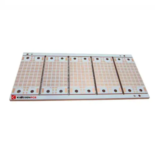
Découpe des matériaux : Le matériau de coupe est la grande surface (48 pouces * 42 pouces) de matière première qui est découpée pour former le panneau de travail dont les fabricants de PCB ont besoin.

Couche intérieure : The inner layer of the circuit uses positive imaging technology, After developing, etching, and de-filming processes, complete the production of the inner layer of the line.

Oxyde noir : Black Oxide is made before lamination. The main role is to roughen the copper surface and increase the surface contact area with the resin to ensure the quality of lamination.

Lamination : Stack up the inner core and prepreg to press into multilayer board through vacuum pressure machine. And make the tooling holes for the next process.

Drilling: Using CNC drilling machine, through holes are drilled for circuit connections between layers.

Cuivre chimique : Electroless copper is chemically deposited, copper. The method deposits a thin copper layer in the non-conductive substrate so that the through-holes are metallization. Then use the plating method to thicken the hole’s copper thickness to achieve the design purpose.

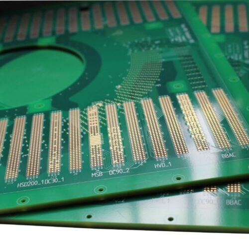
Placage cuivre : Le cuivrage est une méthode de galvanoplastie qui permet d'augmenter l'épaisseur des trous de passage et des surfaces des circuits.

Couche extérieure : Transférer le motif extérieur sur la plaque recouverte de cuivre et graver le cuivre inutile.

Résistance à la soudure Caractère : Impression d'une couche d'encre de masque de soudure isolée sur la surface de la couche externe. Certains circuits imprimés nécessitent également l'impression de symboles sur la couche de masque de soudure.

Surface treatment: Common PCB surface treatments include HASL, OSP, Immersion Gold, ENEPIG, Immersion Silver, Immersion Tin, and Gold finger plating.

Test électrique : All the PCBs must be pen/short tested before outgoing, the test included electrical test and flying probe test. Electrical test for PCB mass production and flying probe test for samples as it’s fast turn round.

Types de fabrication de PCBA

Il existe deux types principaux de fabrication de PCBA : la technologie de montage en surface (SMT) et la technologie de trou traversant (THT).

Technologie de montage en surface (SMT)

L'assemblage de circuits imprimés SMT est une technologie d'assemblage de circuits qui permet de souder des composants à la surface d'un circuit imprimé par refusion ou par immersion. La fabrication de circuits imprimés SMT est généralement utilisée pour les appareils électroniques compacts, légers et à haute densité, tels que les smartphones, les tablettes et les ordinateurs portables.

Technologie des trous de passage (THT)

Through-hole Printed Circuit Board assembly also named DIP involves inserting electronic components through pre-drilled holes in the PCB, and then soldering the leads to the other side of the board. Through-hole Printed Circuit Board assembly is used for heavy-duty electronic devices, such as industrial equipment and high-end audio gear.Most electronic devices are the combination of both SMT and THT assembly methods to achieve a balance between size, weight, and durability.

Caractéristiques de la fabrication des PCBA

Here are some characteristics of PCBA manufacturing

Density Assembly

The Printed Circuit Board assembly can be a high-density, lightweight, and small volume of electronic products. Generally, the volume of electronic products is reduced by 40%-60%, and the weight is reduced by 60%-80% after using the SMT process.

High Reliability

PCBA manufacturing is high reliability, strong vibration resistance, and low solder joint defect rate.

Anti-Interference

PCBA manufacturing has the strong anti-interference ability and better electromagnetic compatibility.

Automation

Most PCBA manufacturing is automated using specialized machinery. This not only increases production efficiency but also ensures consistency and accuracy, and reduces material costs and manpower time.

Materials of PCBA manufacturing

PCBA manufacturing mainly uses three major materials, which are solder paste, flux, and SMT glue.

Solder Paste

Solder paste is made of alloy solder powder and paste flux evenly stirred, it is an indispensable soldering material in the SMT chip processing process, widely used in reflow soldering. Solder paste has a certain viscosity at room temperature, and can be electronic components initially stick in the established position. 

Flux

Flux is the carrier of tin powder, and its composition is basically the same as that of general-purpose flux. In order to improve the printing effect, it is sometimes necessary to add an appropriate amount of solvent, through the action of the activator in the flux.

SMT Glue

SMT glue, also known as SMT adhesive, or SMT red glue, is usually a red (also yellow or white) paste that is evenly distributed with hardeners, pigments, solvents, etc. mainly used to fix the components on the printed board. Generally, we use the method of dispensing or stencil printing to distribute, and then put the components into the oven or reflow oven to heat up and harden.

PCB Manufacturing Fabrication Capabilities

Article Paramètres techniques    spécification
Largeur/espace minimum de ligne de circuit 3/2.7 mil Épaisseur du cuivre fini H oz
Anneau de protection PCB minimum de Via  3 millions  Distance entre le bord du trou et la périphérie de l'anneau 
 Anneau minimum de protection PCB de PTH 5 millions  Distance entre le bord du trou et la périphérie de l'anneau  
 Taille minimale du PCB via la taille 4 millions  Épaisseur du panneau < 1,2 mm 
 Épaisseur minimale du PCB double face 0,2 mm  Épaisseur finale du panneau
Épaisseur minimale du PCB multicouche 0,4 mm Épaisseur finale du panneau
Épaisseur maximale du PCB  8,0 millimètres  Épaisseur finale du panneau 
 Dimension maximale du PCB 609×609 millimètres  PCB simple et double face
 Espace entre la ligne et le bord de la planche 10 millions  Fraisage du contour 
 Couches maximales de PCB 30 couches   
Couleur du masque de soudure PCB Vert, noir, bleu, rouge, blanc, jaune,  
Couleur de sérigraphie PCB Blanc, noir, jaune  
Finition de surface des PCB HASL,ENIG,ENEPIG,ImAg,ImTin,OSP, Hard Gold Plating  
Épaisseur maximale de cuivre de finition 6 onces  
Épaisseur diélectrique 2,5 millions  
Matériau PCB FR-4, substrat en aluminium, Rogers4350C, Polyimide  
Technologie spéciale PCB HDI, via PCB Pad, PCB aveugle et enterré  

How to make PCBA manufacturing?

Article Paramètres techniques    spécification
Largeur/espace minimum de ligne de circuit 3/2.7 mil Épaisseur du cuivre fini H oz
Min rigid PCB Pad Ring of Via  3 millions  Distance entre le bord du trou et la périphérie de l'anneau 
 Min rigid PCB Pad Ring of PTH 5 millions  Distance entre le bord du trou et la périphérie de l'anneau  
 Min rigid PCB Via Size 4 millions  Épaisseur du panneau < 1,2 mm 
 Min rigid PCB Thickness of Double sided 0,2 mm  Épaisseur finale du panneau
Min rigid PCB Thickness of Multilayer 0,4 mm Épaisseur finale du panneau
Max rigid PCB Thickness  8,0 millimètres  Épaisseur finale du panneau 
 Max rigid  PCB Dimension 609×609 millimètres  PCB simple et double face
 Espace entre la ligne et le bord de la planche 10 millions  Fraisage du contour 
 Max rigid  PCB Layers 30 couches   
Rigid PCB Solder Mask Color Vert, noir, bleu, rouge, blanc, jaune,  
Rigid PCB Silkscreen Color Blanc, noir, jaune  
Rigid PCB Surface Finishing HASL,ENIG,ENEPIG,ImAg,ImTin,OSP, Hard Gold Plating  
Épaisseur maximale de cuivre de finition 6 onces  
Épaisseur diélectrique 2,5 millions  
Rigid PCB Material FR-4, substrat en aluminium, Rogers4350C, Polyimide  
Technologie spéciale PCB HDI, via PCB Pad, PCB aveugle et enterré  

How to make PCBA manufacturing?

Solder Paste Printing

Accurately apply solder paste or adhesive onto the PCB pads in preparation for component placement.There are three types solder paste machines: manual printing machines, semi-automatic printing machines and fully automatic printing machines.


Mount

Utilize the equipment-edited program to precisely position the components onto the designated locations of the PCB.The placement machine involves high-speed placement machine and multi-function placement machine.High-speed placement machines are generally used to mount small chip components.The multi-function placement machine is mainly used to mount roll-shaped, disc-shaped or tubular large components or abnormal shape components.

Reflow

Positioned behind the placement machine in the SMT production line, this device creates a heated environment that facilitates the melting of solder paste on the pad. As a result, surface mount components and PCB pads are firmly bonded together using solder paste.

AOI

When AOI is automatically detected, the machine scans the PCB through its camera, automatically collecting images. It then compares the tested solder joints with qualified parameters stored in the database, and checks for defects on the PCB through image processing. Any defects are displayed and marked on the display, allowing maintenance personnel to quickly identify and repair them.

The Application of PCBA Manufacturing

PCBA manufacturing is an important technology that enables the development of complex electronic devices that are used in a wide range of industries and applications. Below are some common applications.

Electronique grand public

PCBA manufacturing is used in a range of consumer electronics, including smartphones, tablets, laptops, televisions, and home appliances.

Automotive

PCBA manufacturing is used in automotive applications for electronic control units, sensors, and other critical components.

Industrial automation

PCBA manufacturing is used in industrial automation applications for controlling machinery, monitoring sensors, and handling data.

Medical equipment

PCBA manufacturing is used in medical equipment for patient monitoring, diagnostics, and treatment.

Aerospace and defense

PCBA manufacturing is used in aerospace and defense applications for controlling and monitoring aircraft systems, satellite communication, and military equipment.

Why choose us?

PCBA manufacturing in King Sun can offer a combination of affordability, quality, and scalability that makes it an attractive option for businesses. There are several advantages of PCBA manufacturing in King Sun.

Low Cost

PCBA manufacturing in King Sun is typically much more cost-effective than in many other factories, due to the lower cost of labor and materials.

High Quality

Despite the lower cost, PCBA manufacturing in King Sun can still be of high quality. We imported production and testing equipment from the United States, Japan, and other countries to help companies improve PCBA manufacturing and testing capabilities.

Large-scale Production

King Sun is one of the largest producers of Printed Circuit boards and PCBA in China, which means that it has the capacity to produce large quantities of circuit boards and PCBA manufacturing quickly and efficiently.

Scalability

King Sun has experience in producing circuit boards for a wide range of applications and industries, including automotive, telecommunications, and consumer electronics. This means that we can scale our production to meet the needs of different clients.

Fast Turnaround

King Sun has our own Printed Circuit Board factory and assembly factory, so the lead times can be very fast than other suppliers, which can be a significant advantage for clients who need their products quickly.