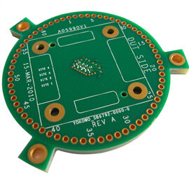
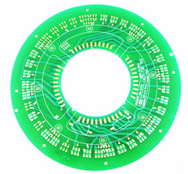
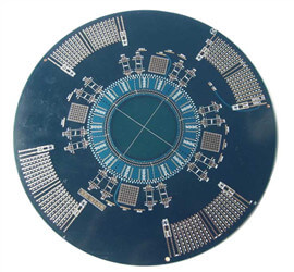
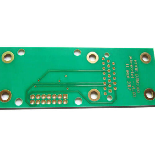
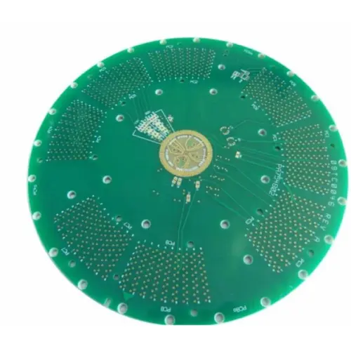
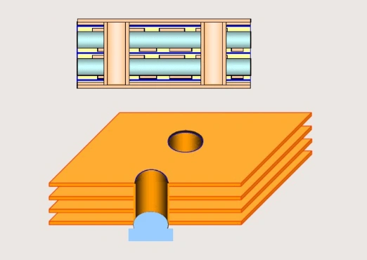
What is HDI PCB?

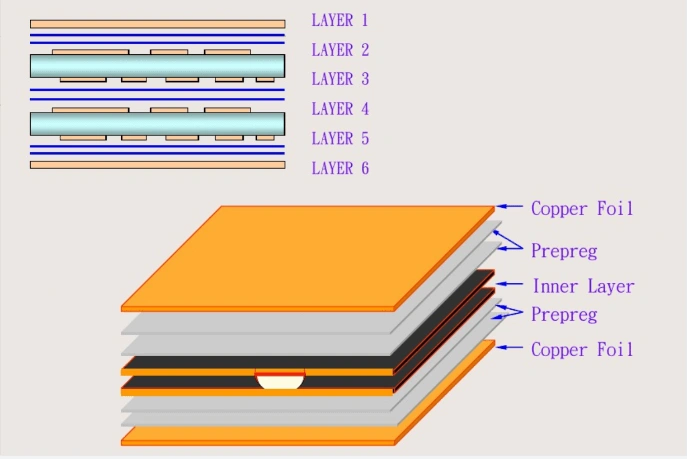
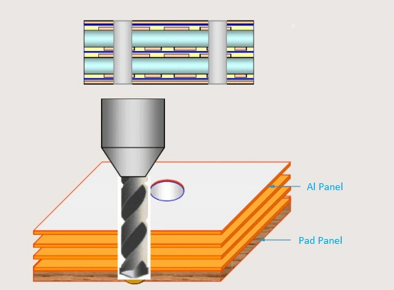
HDI PCB is the abbreviation of high density interconnector PCB. HDI PCB manufacturer makes the HDI board by increased layers through micro-blind&buried vias.

HDI PCB board is a compact product specially designed for small capacity users.

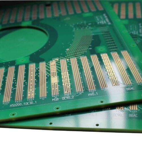
The HDI board includes the following via types:

Microvia PCB: In the PCB industry, vias with a diameter of less than 150um (6mil) are called microvias.

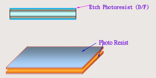
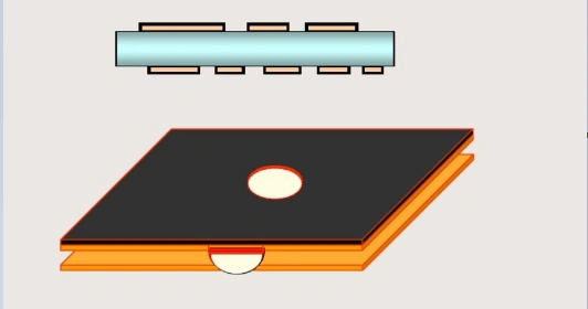
Buried vias: The vias are buried in the inner layer, generally not visible in the finished product. 

Blind vias: The blind vias are drills from top layer or bottom layer to a certain inner layer. They are not through the whole HDI board. 

Characteristics of HDI PCB Board

Smaller and Lighter

HDI PCB manufacturer make the HDI PCB board through continuous lamination and laser drilling with a large number of micro-buried blind holes. So it has the advantages of being light, thin, short, and small.

High density

High density interconnect PCB design with more vias, traces, copper pads and inner layers. The via diameter is usually less than 150um, the line width and line spacing do not exceed 76.2um, also the thickness of the interlayer dielectric is less than 80um.

Better Electrical Performance

HDI PCB boards have better electrical performance due to multiple pressing and plating. In addition, the HDI PCB board has better improvement for radio frequency interference, electromagnetic wave interference, electrostatic discharge, heat conduction, etc.

High Requirements For Plug Vias

At present, HDI PCB board buried& blind vias plugging technology is painful for HDI PCB manufacturer. Quality problems will involve vias cavity,uneven dielectric thickness and uneven board edge if HDI PCB manufacturer does not do well with buried and blind vias.

Features of HDI PCB Board Manufacturing

The HDI PCB manufacturing process is usually different from that of other standard PCBs, The following are some special characteristics of HDI PCB board manufacturing.

Multiple Laminations

Lamination of PCB core board, PP and copper foil. Unlike other standards PCBs, HDI PCB boards go through the lamination process multiple times. These continuous laminate structures help prevent movement and breakage during drilling.

Via in pad Technology

HDI PCB with via in pad technology is that the via be drilled in copper pad and filled with resin or copper materials. Then plating a layer copper to cover the via, so the pad can be used in soldering.

Filling vias Types

Via filling type should generally be determined based on specific application and PCB requirements. Filling materials used include chemical plating, silver filling, copper filling, conductive resin, and non-conductive resin. The most common via filling material is a non-conductive resin.

Laser Drilling Technology

Laser drilling is widely used in HDI PCB design. The laser heads can produce laser light up to 20 microns in diameter. It’s easy to cut metal and fiberglass and produce very small and clean vias. Using smooth glass fibers with a lower dielectric constant allows for smaller vias.

Capacités de fabrication

Article Paramètres techniques    spécification
Largeur/espace minimum de ligne de circuit 2.7/2.7 mil Épaisseur du cuivre fini H oz
Anneau de protection PCB minimum de Via  3 millions  Distance entre le bord du trou et la périphérie de l'anneau 
 Anneau minimum de protection PCB de PTH 5 millions  Distance entre le bord du trou et la périphérie de l'anneau  
 Taille minimale du PCB via la taille 3 millions  Épaisseur du panneau < 1,2 mm 
 Min PCB Thickness of 4 Layer 0,4 mm  Épaisseur finale du panneau
Épaisseur minimale du PCB multicouche 0,4 mm Épaisseur finale du panneau
Épaisseur maximale du PCB  3.2 mm  Épaisseur finale du panneau 
 Dimension maximale du PCB 609×450 mm  PCB simple et double face
 Espace entre la ligne et le bord de la planche 10 millions  Fraisage du contour 
 Couches maximales de PCB 40 Layer   
Couleur du masque de soudure PCB Vert, noir, bleu, rouge, blanc, jaune,  
Couleur de sérigraphie PCB Blanc, noir, jaune  
Finition de surface des PCB HASL,ENIG,ENEPIG,ImAg,ImTin,OSP, Hard Gold Plating  
Épaisseur maximale de cuivre de finition 2 oz  
Épaisseur diélectrique 2,5 millions  
Matériau PCB FR-4, substrat en aluminium, Rogers4350C, Polyimide  
Technologie spéciale Countersink hole, Via in Pad PCB,Blind&Buried PCB  

Types of HDI PCB


Stackup 1+N+1

There is and only one blind& buried drill that directly connects two adjacent layers. For example, layer 1 and layer 2 are connected or layer X is connected to layer (X-1).

Stackup 2+N+2

The blind hole from the outer layer of the via hole to the third layer can be directly connected to the 1-3 layer, or it can be connected to the 1-2 layer and the 2-3 layer separately.

Anylayer

There are micro-vias connections between any adjacent layers. For example, L1-L2,L2-L3,L3-L4,L4-L5,L5-L6,L6-L7,L7-L8… etc.

HDI PCB Manufacturing Process

Inner Layer

The first step is cut material sheet into working panel, then start to make Inner Layer that uses dry film to transfer PCB pattern to the copper clad by exposure and development processes.

King Sun PCB’s inner layer production capability is presently 3mil line/3mil space for Hoz and 1oz copper.

Black Oxide Coating

Black oxide makes core to have a uniform fluff layer that increases the bond strength between the copper foil and prepregs. It also removes grease and burs from the material surface to ensure cleanliness before lamination.

Inner Layer Lamination

This lamination is made for blind vias and buried vias layers. The first step is stack and fix the prepreg sheet and the oxidized inner layer board in position. Then laminated the copper foils, prepregs and inner layer through automatic pressing machine. 

Some HDI PCBs are multiple laminations for different PCB blind&buried vias designs.

Stackup 1+N+1: This HDI PCB type is one time lamination.

Stackup 2+N+2: This HDI PCB type is twice laminations.

Stackup Anylayer: This HDI PCB type is multiple laminations.

Inner Layer Drilling(blind and buried vias)

After first lamination, then blind vias and buried vias will be drilled.

When the via diameter is more than 0.2mm, we will use traditional CNC drilling machine.When the via diameter is less than 0.2mml, we will use laser drilling.

Inner layer Plating

After blind vias and buried vias be drilled, the vias need to be plated before outer layer lamination. Board thickness and via diameter aspect ratio is not more than 10 to ensure the via wall plating is good.

Outer layer Lamination

The next PCB manufacturing processes are as same as standard multilayer PCB.

The Application of HDI PCB

  • Mobile communication devices and notebook computers. Moreholes, light weight, small size, strong function.
  • Computer and network communication equipment and large equipment. Few holes, high layer acounts, impedance control for transmitted signal trace.
  • Chip carriers for LSI packaging, including pads and flip chips, etc.Small line width and spacing (generally less than 2 mils), high precision, small aperture (1-2 mils), small aperture spacing (≤5 mils), good heat resistance, and small thermal expansion coefficient of the substrate.

Pourquoi nous choisir?

Quick Turn PCB Fabrication

We can make PCB prototypes with a very fast turnaround lead time:

Nombre de couches Délai de livraison standard Retour rapide
1-2 Couche 4-5 JOUR 24 heures
4 couches 5-6 JOUR 48 heures
 6 couches 7-8 JOUR 96 heures
 8 couches 9-10 JOUR 140 heures
 10 Layer 10-12 DAY 192 Hours
 
Technologies de PCB complexes

We make very complex and special PCBs like below:

  • Via in Pad PCB
  • PCB de pièce de monnaie en cuivre intégré
  • Backdrill PCB
  • Depth Slot PCB
  • Countersink Hole PCB
  • Blind and buried vias PCB