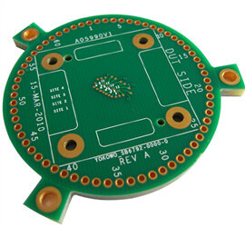
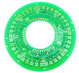
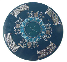
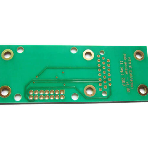
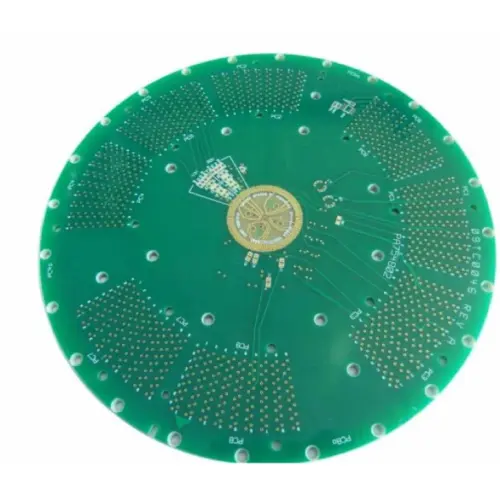
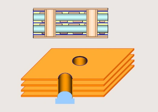
What is HDI PCB?

HDI PCB is the abbreviation of high density interconnector PCB. HDI PCB manufacturer makes the HDI board by increased layers through micro-blind&buried vias.

HDI PCB board is a compact product specially designed for small capacity users.

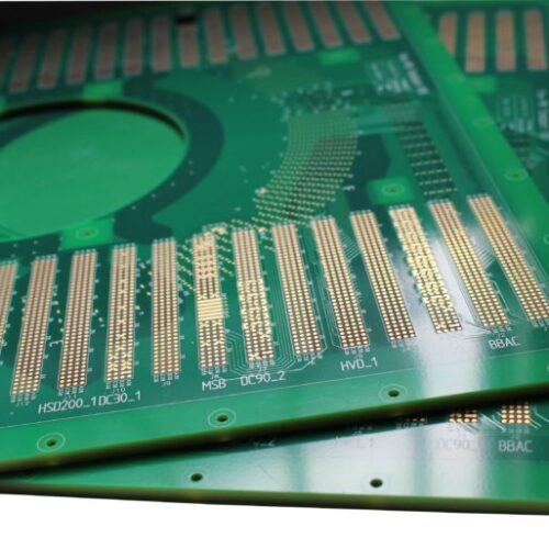
The HDI board includes the following via types:

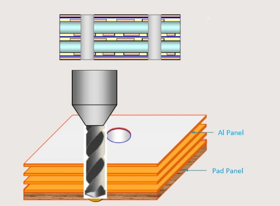
Microvia PCB: In de PCB-industrie worden via's met een diameter van minder dan 150um (6mil) microvia's genoemd.

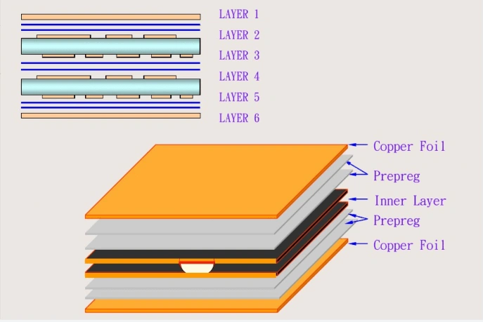
Begraven via's: De via's zijn begraven in de binnenste laag en zijn doorgaans niet zichtbaar in het eindproduct. 

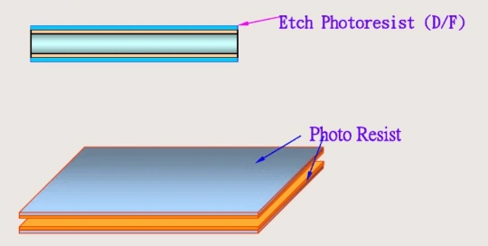
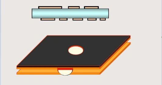
Blind vias: The blind vias are drills from top layer or bottom layer to a certain inner layer. They are not through the whole HDI board. 

Characteristics of HDI PCB Board

Kleiner en lichter

HDI PCB manufacturer make the HDI PCB board through continuous lamination and laser drilling with a large number of micro-buried blind holes. So it has the advantages of being light, thin, short, and small.

Hoge dichtheid

High density interconnect PCB design with more vias, traces, copper pads and inner layers. The via diameter is usually less than 150um, the line width and line spacing do not exceed 76.2um, also the thickness of the interlayer dielectric is less than 80um.

Betere elektrische prestaties

HDI PCB boards have better electrical performance due to multiple pressing and plating. In addition, the HDI PCB board has better improvement for radio frequency interference, electromagnetic wave interference, electrostatic discharge, heat conduction, etc.

Hoge eisen aan stekkervia's

At present, HDI PCB board buried& blind vias plugging technology is painful for HDI PCB manufacturer. Quality problems will involve vias cavity,uneven dielectric thickness and uneven board edge if HDI PCB manufacturer does not do well with buried and blind vias.

Features of HDI PCB Board Manufacturing

The HDI PCB manufacturing process is usually different from that of other standard PCBs, The following are some special characteristics of HDI PCB board manufacturing.

Meerdere lamineringen

Lamination of PCB core board, PP and copper foil. Unlike other standards PCBs, HDI PCB boards go through the lamination process multiple times. These continuous laminate structures help prevent movement and breakage during drilling.

Via inpad-technologie

HDI PCB with via in pad technology is that the via be drilled in copper pad and filled with resin or copper materials. Then plating a layer copper to cover the via, so the pad can be used in soldering.

Vullen via soorten

Via filling type should generally be determined based on specific application and PCB requirements. Filling materials used include chemical plating, silver filling, copper filling, conductive resin, and non-conductive resin. The most common via filling material is a non-conductive resin.

Laserboortechnologie

Laser drilling is widely used in HDI PCB design. The laser heads can produce laser light up to 20 microns in diameter. It’s easy to cut metal and fiberglass and produce very small and clean vias. Using smooth glass fibers with a lower dielectric constant allows for smaller vias.

Fabricagemogelijkheden

Item Technische parameters    Specificatie
Min. breedte/ruimte circuitlijn 2,7/2,7 miljoen Afgewerkte koperdikte H oz
Min. PCB-padring van Via  3 miljoen  Afstand tussen de rand van het gat en de buitenrand van de ring 
 Min PCB-padring van PTH 5 miljoen  Afstand tussen de rand van het gat en de buitenrand van de ring  
 Min. PCB via grootte 3 miljoen  Plaatdikte < 1,2 mm 
 Min. PCB-dikte van 4 lagen 0,4 mm  Dikte van de uiteindelijke plaat
Min. PCB-dikte van meerlaags 0,4 mm Dikte van de uiteindelijke plaat
Maximale PCB-dikte  3,2 mm  Dikte van de uiteindelijke plaat 
 Maximale PCB-afmeting 609×450mm  Enkel- en dubbelzijdige printplaat
 Ruimte tussen lijn en bordrand 10 mil  Frezen van omtrek 
 Maximale PCB-lagen 40 laag   
PCB-soldeermaskerkleur Groen, Zwart, Blauw, Rood, wit, Geel,  
PCB zeefdruk kleur Wit, zwart, geel  
PCB-oppervlakteafwerking HASL,ENIG,ENEPIG,ImAg,ImTin,OSP, hard vergulden  
Maximale afwerking koperdikte 2 oz  
Diëlektrische dikte 2,5 miljoen  
PCB-materiaal FR-4, aluminiumsubstraat, Rogers4350C, polyimide  
Speciale technologie Verzonken gat, via in Pad PCB, Blind & Buried PCB  

Soorten HDI-printplaten


Stapel 1+N+1

Er is slechts één blinde en ingegraven boor die twee aangrenzende lagen rechtstreeks met elkaar verbindt. Laag 1 en laag 2 zijn bijvoorbeeld met elkaar verbonden of laag X is verbonden met laag (X-1).

Stapelopstelling 2+N+2

Het blinde gat van de buitenste laag van het via-gat naar de derde laag kan rechtstreeks worden verbonden met de 1-3-laag, of kan afzonderlijk worden verbonden met de 1-2-laag en de 2-3-laag.

Elke laag

Er zijn micro-via-verbindingen tussen aangrenzende lagen. Bijvoorbeeld L1-L2,L2-L3,L3-L4,L4-L5,L5-L6,L6-L7,L7-L8... enz.

HDI PCB-productieproces

Binnenste laag

The first step is cut material sheet into working panel, then start to make Inner Layer that uses dry film to transfer PCB pattern to the copper clad by exposure and development processes.

King Sun PCB’s inner layer production capability is presently 3mil line/3mil space for Hoz and 1oz copper.

Zwarte oxidecoating

Black oxide makes core to have a uniform fluff layer that increases the bond strength between the copper foil and prepregs. It also removes grease and burs from the material surface to ensure cleanliness before lamination.

Laminering van de binnenlaag

This lamination is made for blind vias and buried vias layers. The first step is stack and fix the prepreg sheet and the oxidized inner layer board in position. Then laminated the copper foils, prepregs and inner layer through automatic pressing machine. 

Some HDI PCBs are multiple laminations for different PCB blind&buried vias designs.

Stackup 1+N+1: Dit HDI-PCB-type is eenmalig gelamineerd.

Stackup 2+N+2: Dit HDI PCB-type is tweemaal gelamineerd.

Stackup Anylayer: This HDI PCB type is multiple laminations.

Boren in de binnenlaag (blinde en begraven via's)

After first lamination, then blind vias and buried vias will be drilled.

When the via diameter is more than 0.2mm, we will use traditional CNC drilling machine.When the via diameter is less than 0.2mml, we will use laser drilling.

Binnenlaag Plating

After blind vias and buried vias be drilled, the vias need to be plated before outer layer lamination. Board thickness and via diameter aspect ratio is not more than 10 to ensure the via wall plating is good.

Buitenlaag Lamineren

The next PCB manufacturing processes are as same as standard multilayer PCB.

De toepassing van HDI-PCB's

  • Mobile communication devices and notebook computers. Moreholes, light weight, small size, strong function.
  • Computer and network communication equipment and large equipment. Few holes, high layer acounts, impedance control for transmitted signal trace.
  • Chipdragers voor LSI-verpakkingen, inclusief pads en flipchips, enz. Kleine lijnbreedte en -afstand (doorgaans minder dan 2 mil), hoge precisie, kleine opening (1-2 mil), kleine openingafstand (≤5 mil), goede warmte weerstand en kleine thermische uitzettingscoëfficiënt van het substraat.

Waarom voor ons kiezen?

Snelle PCB-fabricage

We kunnen PCB-prototypes maken met een zeer snelle doorlooptijd:

Aantal lagen Standaard doorlooptijd Snel omdraaien
1-2 laag 4-5 DAG 24 uur
4 lagen 5-6 DAG 48 uur
 6 lagen 7-8 DAG 96 uur
 8 lagen 9-10 DAG 140 uur
 10 laag 10-12 DAG 192 uur
 
Complexe PCB-technologieën

Wij maken zeer complexe en speciale PCB’s zoals hieronder:

  • Via in Pad-PCB
  • Ingebouwde koperen muntprintplaat
  • Achterboren printplaat
  • Dieptesleuf-printplaat
  • PCB met verzonken gat
  • Blinde en ingegraven via's PCB