Introduction:
Chip On Board (COB) technology has reached a state of stability within the electronics manufacturing sector. In the past, people used COB to produce less expensive consumption goods. COB is more suitable than IC for use in confined spaces as electronic devices continue to shrink in size. In this post, we will discuss chip-on-board in depth.
Understanding Chip on Board PCB
A printed circuit board with a chip on board is a packaging method. The electronic parts can be assembled on a printed circuit board by chip on board. This method connects bare integrated circuits on the board’s surface. Moreover, it does not need to configure individual components.
The chip on the board helps make electronic devices lighter and smaller. These methods, such as ceramic or plastic packaging, differ from the old ones.
You can achieve compact and efficient assembly of the chips by using solder cracks or adhesives for chip mounting. When the semiconductor is bound to the board, it creates shorter electrical paths. This improves electrical performance and reduces signal losses. It helps manage heat well by connecting chips to thermal pads or heat sinks on the board.
How Chip-On-Boards Are Made?
Substrate preparation:
They use a clean board to prepare the printed circuit board. Then, add a sticky layer of conductive material to create the area where the chips will stick.
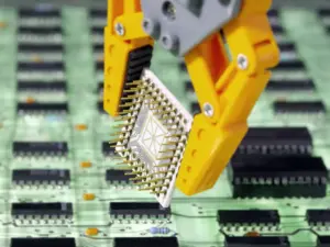
Die attach:
Place the uncoated chips on the area of the board coated with adhesive. Specialized instruments or pick-and-place devices are used for this procedure.
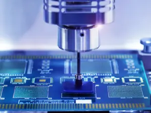
Bonding:
Chips are configured by using solder ridges. These solder ridges adhere to a board. This linkage connects the chip’s contact areas and the board’s conductive traces.
Wire bonding:
Under certain conditions, fine wires connect bonding pads to board traces via wire bonding. This procedure facilitates electrical signal transmission between the board and the chip.
Encapsulation:
You can cover the entire assembly in an encapsulant material. It protects chips and wire bonds from external components. Additionally, it reveals the epoxy coating.
Testing:
Testing techniques are applied during COB assembly. It ensures the functionality and reliability of COB. Processes are executed, including electrical testing, visual inspection, and temperature cycling. These steps confirm the operation of COB.
Final Assembly:
After completing all testing steps, the chip on board assembly becomes ready for integration into the electronic devices. It is not limited to smartphones and LED chip on board lighting.
Main Advantages of Chip-On-Board
- Chip on board has a compact design. Mounting the bare semiconductor chips onto a substrate via COB produces space-efficient solutions. This attribute is beneficial in situations where restrictions on dimensions are critical.
- COB technology is distinguished by its increased dependability. COB ensures resilient performance. It provides high-pressure environments by chance of wire bonding failures and other potential risks. This resilience is critical for applications where delay is unacceptable. These are industrial controls and automotive electronics.
- COB has thermal control functionalities. Adding circuits to the base cools it down, making it suitable for electronics and LED lights that need power.
- Large-scale production can yield economic benefits. Eliminating packaging material needs and optimizing the assembly process. Compared to ICs, it could keep costs low.
Disadvantages of Chip On Board (COB) LEDs
- Substrate attachment and sealing of the semiconductor device. It impedes the ability to replace or enhance components. This inflexibility may present difficulties in circumstances that need the ability to adjust.
- It contributes to the manufacturing process’s complexity. COB technology is more challenging to set up and use than traditional IC packaging methods. This is because it requires particular tools and skills. This intricacy may contribute to increased upfront expenses and extended production lead times.
- Because of the specialized materials and devices needed, COB technology may incur a high initial cost. However, large-scale production experiences financial benefits. However, smaller-scale initiatives or prototypes may find the initial investment costly.
Applications of Chip On Board
Automotive Electronics:
Automotive sensors and control units use COB technology. They have durability and resistance to environmental conditions.
Medical Devices:
Medical devices often rely on COB technology. It has compact dimensions and reliable characteristics.
LED Lighting:
People use chip-on-board lighting in applications. It has high luminosity, reliable operation, and compact design.
Industrial Controls:
Due to its thermal performance and durability, industrial control systems and automation tools use COB.
What are Chip On Board Led Lights?
“Chip on board LED” refers to the direct attachment of LED circuits to a substrate composed of sapphire or silicon carbide. This process creates LED arrays. The chip on board LED is a more recent and sophisticated entrant to the market. They offer many significant benefits in comparison to the previous LED technology.
PCB chipped technology demonstrates an increased lumen density. Older LED iterations use only one DIP or three SMD LEDs, accomplished through many diodes. An increased number of diodes in an LED will result in more consistent and intense light and reduced space required. COB technology simplifies LEDs using a single circuit design featuring two contacts when the number of diodes on the semiconductor is irrelevant.
Design Consideration for Chip-On-Board PCBs
A semiconductor die featuring exposed contacts is soldered to the printed circuit board using the chip on board method.
Furthermore, there is no interposer, substrate, or lead frame (which is required for wire bonding). After sticking the chip, it can be covered with epoxy on the PCB to protect it and the wire-bonded pads.
In the placement and mounting of chip on board in a standard printed circuit board, there are two prevalent approaches:
PCB Layout
An integrated PCB editor and a connection to many domains in real-time.
- Direct wire bonding between the die and the PCB.
- In flip-chip assembly, the chip is attached like a BGA.
After attaching and assembling, manufacturers encase the chip in an epoxy or conformal coating. You can cure these coatings either thermally or ultravioletly. The most critical design element in the PCB layout is the footprint that facilitates die attachment to the PCB.
Flip-Chip
A flip chip is an unencapsulated component affixed to a PCB like a BGA fan-out. Underfill encapsulates the solder junctions from excessive mechanical stress, a crucial element. The PCB laminate may consist of FR4-grade standard material, flex, PTFE, or other specialized material.
With this approach, the footprint should be crafted like a BGA footprint. However, the assembly process will be unique. FCOB involves fluxing the solder onto the PCB; the solder does not adhere to the die. The chip will be refilled in the same manner as other SMD components after being positioned. So, some footprint-based DFA is required to ensure reliable assembly.
The exposed pad size must be adjusted to fall within the typical range used in a BGA by utilizing the solder mask and paste mask. Use the solder mask as a dam (SMD pad) if the bump pitch is sufficient to create large solder mask slivers. Use an NSMD pad otherwise to prevent solder mask slivers from separating between ridges.
Wire Bonding
A die-attached pad is affixed to the PCB. Wire connections are established through the contact areas on the die and the pads that encircle the chip. It is recommended to encapsulate the wire connections and die in this design with epoxy. This will protect them against environmental exposure. This will protect the conductors against corrosion and mechanical damage.
High-Speed PCB Design
The pads are excessive when the footprint for the wire bonding pads in the PCB is generated. The footprint requires consideration of the following parameters:
- Contact pad shape
- Contact pad size
- Contact pad pitch
Rectangular pads might be the same size as those used in the part after it has been packed, like in a QFN or LQFP package. However, the square pads are also acceptable. The breadth of the contact spheres utilized to link a wire to the PCB will be between 20 and 30 microns.
The contact pad width ranges from 50 to 150, and we compute the pad pitch using the same value. By using the pad pitch and sizing values, you can arrange a variety of pads within the PCB footprint to assist the wire bonds.
Conclusion
Chip on board technology has changed the electronics industry. It provides advantages over traditional packaging methods. Due to the direct bonding, electronic devices with chips directly bonded on board are smaller, lighter, and more efficient.
Eliminating excess packaging and reducing electrical paths achieve excellent electrical performance. It has minimal signal losses and effective thermal management. This method is vital for creating small and advanced technologies in different industries. It is essential for making electronic parts smaller.
It offers a variety of applications and is used as a chip on board lighting systems, automobile applications, and mobile phone devices.