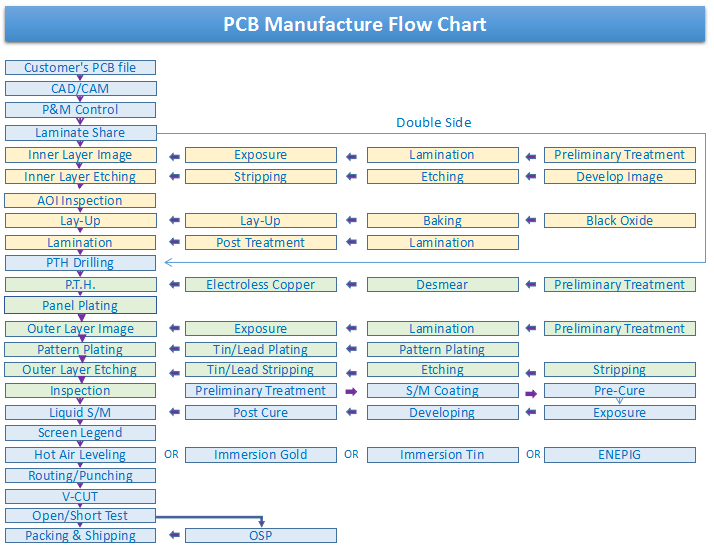
What is the PCB Manufacturing Process?

The full name of the PCB is the printed circuit board. It is manufactured through a printing process.
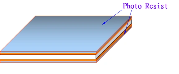
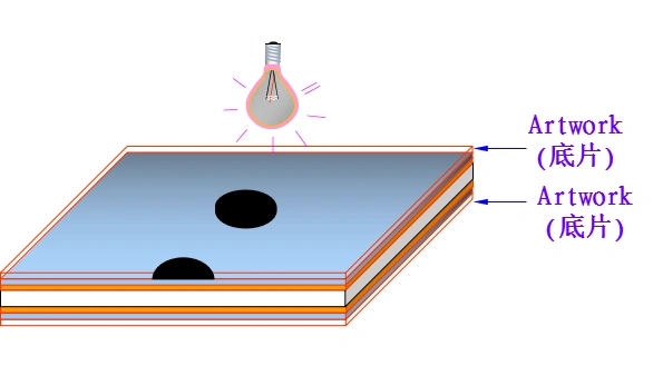
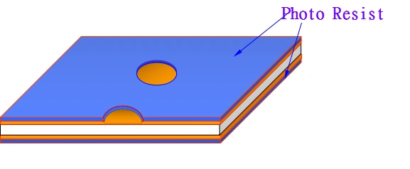
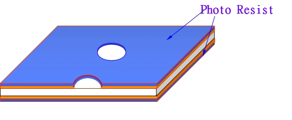
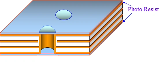
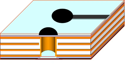
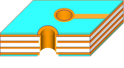
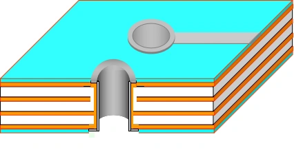
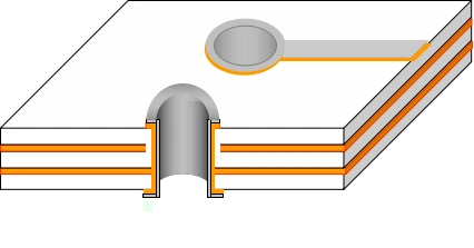
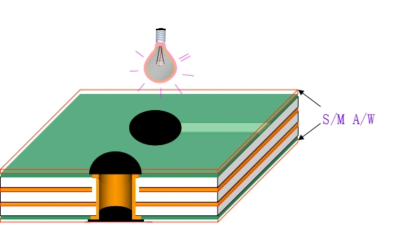
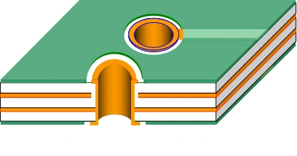
PCB manufacturing involves transferring the PCB graphic onto a copper-clad board. This is done according to the designed circuit pattern.

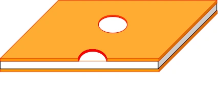
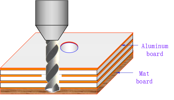
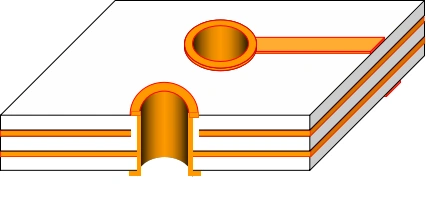
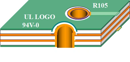
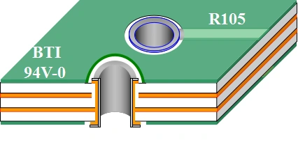
Then, metalize the through holes and print solder mask ink to protect the copper foil and traces.

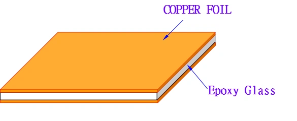
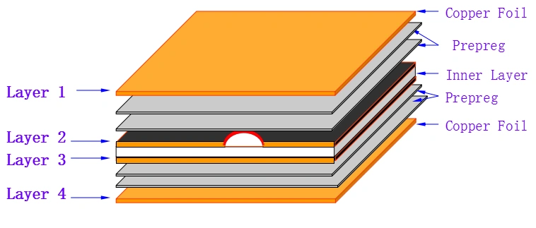
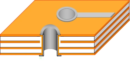
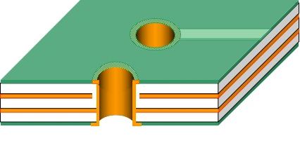
Finally, the exposed pads are surface-treated to form the required circuit board. The circuit board’s raw material is copper-clad laminate. It’s an insulating board with a thin layer of copper foil.

A printed circuit board is the platform for attaching electronic components. It also provides a way for these components to communicate. This creates an electrical conduction pathway.

PCB manufacturing Process Flow Chart:

PCB manufacturing Process Flow Chart

PCB Manufacturing Processes

(i) Lnner Layer

Step 1: Preliminary Treatment

Removes the anti-tarnish coating, dirt, and grease from the copper-clad laminate.

Step 2: Dry Film Lamination

Application of an UV sensitive dry film to cleaned surface of the copper laminate. Using a fully automated slice laminator (CSL). It applies a dry film to both sides of the copper laminate using heat and pressure. The line includes material finishing, CSL, loaders and stackers.

Step 3: Dry Film Exposure

A negative phototool or artwork is imaged onto dry film on both sides of the copper clad by UV light. This leaves a positive image in the dry film.
During exposure, the UV energy is absorbed by the dry film directly under the clear areas of the artwork. This causes it to polymerize and harden. The film under the dark areas of the artwork remains soft.

Step 4: Dry Film Developing

After the dry film is imaged, the unexposed soft areas dissolve. The hardened dry film remains unaffected.

Step 5: Copper Etch

The remaining hardened dry film on the copper acts as a “resist.” The unprotected copper is chemically dissolved or etched.

Step 6: Strip Resist

The hardened dry film is stripped from the copper. This leaves the desired copper pattern, copied from the artwork. The inner-layer image transfer process is done.

Step 7: Automated Optical Inspection(AOI)

We inspect inner-layer cores with a computer-aided optical inspection system. It finds any pattern defect from the image transfer process. The AOI process uses a data file from CAM. The machine compares the scanned image to a computer file. AOI benefits include:
– Early detection of process deviations
– Reduction of final test fallout
– Consistent line width and tolerances

Step 8: Inner-layer Oxide

This process intentionally creates a coating of copper oxide on the copper circuitry. It will enhance the surface topography.

This will increase the bond strength between the core and the bonding materials in the multi-layer lamination.

Step 9: Vacuum Press Lamination

Inner-layer oxidized cores are stacked with prepreg and copper foils. This depends on the type of build.

PCB Board Manufacturing Process

(i) Out Layer

Step 1: NC Drilling

Panels from the vacuum press will be drilled to interconnect the circuit’s layers. The drills are CNC-controlled. They get files from CAM. The files show the number of hits, hole sizes, and the drill’s path.

Panels from the lamination presses are first routed and edge beveled to clean up the edges of panels. The tooling holes are spot-faced to allow the panels to lie flat on the drill table.

Step 2: Electroless Copper

It’s a chemical metalization process. It’s meant to metalize the surface of dielectric material at the hole wall. It makes an electrical connection between all exposed copper surfaces.

The process deposits a very thin (75 micro-inches), fragile coating of pure copper on the panel’s full surface. This includes the drilled hole walls and the external surfaces.

Step 3: Dry Film Lamination

Just as in ithe nner layer, photosensitive ddry filmis laminated on both sides of the panel.

Step 4: Dry Film Exposure

The positive image creates a negative (reverse) image of the external circuit on the dry film. The dark areas of the artwork cover the panel holes. The film and the artwork are exposed to UV light, and the external image is created.

Step 5: Dry-Film Developing

The unexposed areas of the dry film are dissolved. The dry film creates a “channel” for copper pattern plating.

Step 6: Copper and Tin Plating

Copper plating is electrodeposited onto the copper foil that is outlined by the dry film. Copper is plated on the surface and in the holes of the panel. The panels are suspended in an acid-copper bath with copper anode balls.

Current from a DC rectifier drives copper to be consumed from the anodes. It is then deposited on the plated surfaces. Organic compounds are also introduced to the plating baths to control deposition rates.

Immediately after copper plating, the surface of the copper is electroplated with a thin layer (0.003″) of tin. This is copper plating. Tin will act as ean tch resist in auture manufacturing pprocesses

Step 7: Dry Film Strip

The plating resist is removed, exposing the base copper underneath. The plated copper remains protected by the tin plating etch resist.

Step 8: Copper Etch

We remove the exposed copper through etching. The plated tin is a resist, protecting the plated copper from the etchant.

Step 9: Tin Strip

The tin plate etch resist is stripped off, and the external circuitry is exposed.

Step 10: Soldermask

Solder mask is an insulative protective coating. It is applied to the external circuitry after the SES process.

Step 11: Solder mask Exposure

PISM acts like a Dry Film. Negative artwork is used to create the image of the solderable areas, such as SMT pads and PTH. The solder mask is exposed to UV light in a controlled environment, such as the inner or outer layer.

Step 12: Soler mask Developing

The unexposed PISM is developed away, leaving the solderable pads exposed.

Step 13: Silkscreens(Idents)

After the board finish is applied, we add the legends to the panel through screen printing. The identification ink which is available in different colors, UV or thermally cured.

Step 14: Solderable Finishes

The most common finishes are Hot Air Solder Leveler (HASL), ENIG, and OSP. They are used because of their good electrical and mechanical properties, excellent shelf life, and continuity.

 NC Routing

– Individual boards are cut from the manufacturing panel

– Use an NC Router, similar to NC Drilling equipment

– Typically 0.093” cutting tool(0.030”,0.062”)

 Q.C. Inspection

– 100% electrical test for open circuit, short circuit

– Universal test equipment with customized fixtures

– Double-sided access

– Test to electrical netlist generated from Gerber data

– Detect any cosmetic defects according to IPC-A-600.
(i.e., scratches, chips, uneven solder)

– Rework: solder mask touch-up, solder touch-up

– Typically 100% inspection

– Verification of all dimensions:

  • Registration
  • Annular Ring
  • Board Thickness
  • Warp & Twist

– Review product to customer specification
– Measurement of all metalization thicknesses(Cu, SN/PB, Au, Ni)
– Special Requirements(cleanliness, microsection, TDR)