-gallery-770x578-1-500x500.jpg)
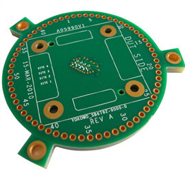
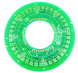
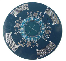
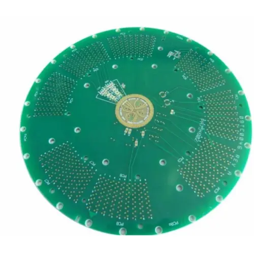
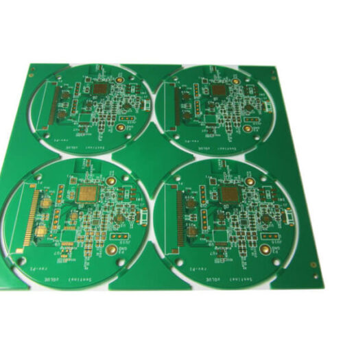
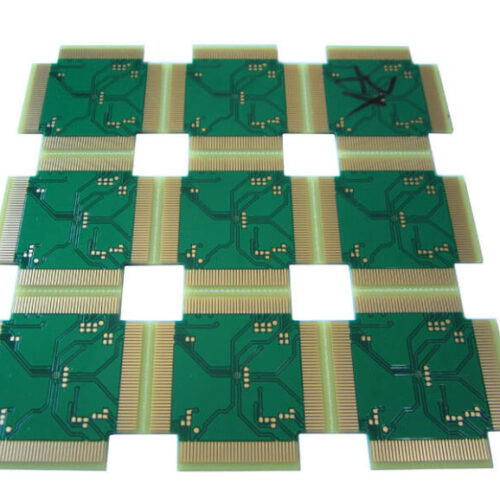
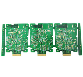
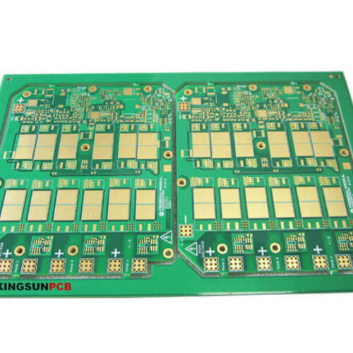
What is a HDI board?
HDI stands for High Density Interconnect. The technology used in printed circuit board (PCB) manufacturing allows for a higher concentration of electronic components and interconnections in a smaller area.
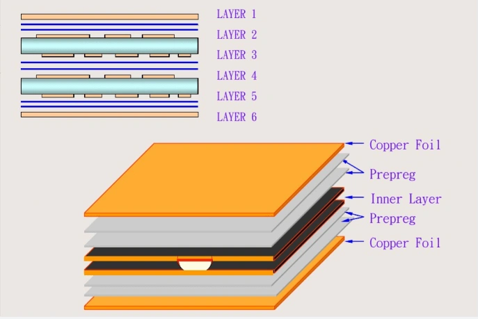
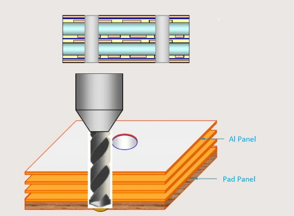
The HDI PCB manufacturer makes the HDI board by increasing layers through micro-blind and buried vias. This technology is commonly used in compact electronic devices such as smartphones, tablets, and wearable devices, where space is a premium.
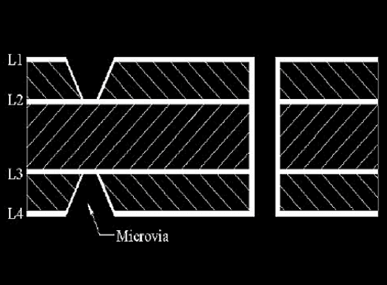
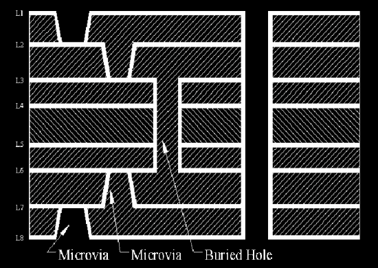
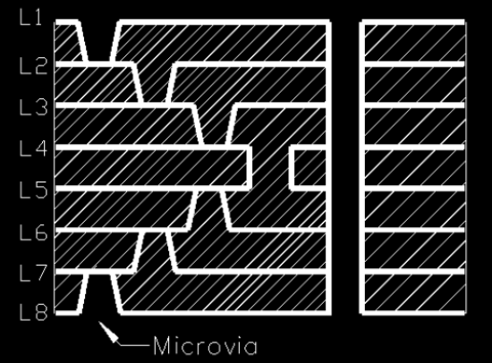
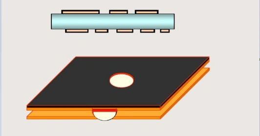
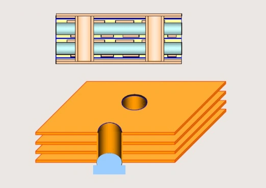
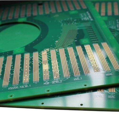
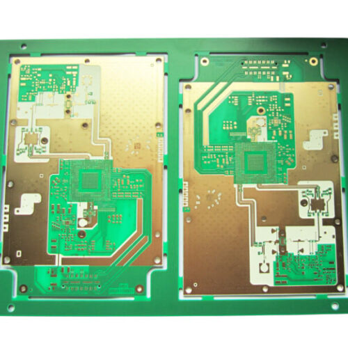
The HDI board includes the following visa types:
- Microvia PCB: In the PCB industry, vias with a diameter of less than 150um (6mil) are called microvias.
- Buried vias: The vias are buried in the inner layer, generally not visible in the finished product.
- Blind vias: The blind vias are drills from a top layer or bottom layer to a certain inner layer. They are not through the whole HDI board.