ENEPIG PCB Technology
ENEPIG is the abbreviation of Electroless Nickel Electroless Palladium Immersion Gold. It’s a PCB board surface finish. Some engineers also call it ENIPIG. Do you know the difference between them?
ENEPIG and ENIPIG are immersed in a palladium layer between the nickel and gold layers. This can prevent the mutual migration between nickel and gold, and no black pad will appear.
They all have strong wire bonding ability, good solder joint reliability, the ability to withstand multiple reflow soldering, excellent storage time, etc. They can correspond to and meet a variety of different assembly requirements.
The difference lies in the thickness of the plating. If thin palladium (replacement palladium) has a thickness of 0.0125-0.02um (0.5-0.8u”), we call it ENIPIG. If thick palladium has a thickness of 0.05-0.5um (2-20u”), we call it ENEPIG.
Feature of ENEPIG
- ENEPIG plating can be used for both gold and aluminum wire bonding.
- ENEPIG PCB finish has excellent solderability, even after high-temperature aging and high humidity.
- The palladium layer separates the nickel and gold layers, preventing the mutual migration between gold and nickel. There will be no ENEPIG black pad phenomenon.
- The ENEPIG finish cost is cheaper than hard gold plating, the thickness of gold is 0.03~0.05um, and the average palladium thickness is about 0.05~0.1.um.
- The ENEPIG thickness is thin and well-proportioned.
- The compatibility between the ENEPIG finish and the solder paste is very good.
- The nickel layer is lead-free of ENEPIG plating.
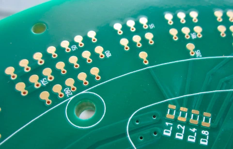
- Very suitable for SSOP, TSOP, QFP, TQFP, PBGA, and other package components.
ENEPIG deposition process
1. Oil Removal
Like other surfaces, Oil removal is the first important surface treatment process. Remove mild oil and oxides on the copper surface, clean the copper surface, and increase wettability.
Feature requirements:
- Generally acid degreaser
- No damage to solder resist ink
- Low foam type, easy to wash
2. Micro Etching
Microetching is surface roughening. It can remove the oxide layer on the surface of copper foil, and etch away 1um~2um copper from the surface of copper substrate. Increase the adhesion between copper and chemical nickel layer.
3. Acid Cleaning
The method of using an acid solution to remove scale and rust on the copper surface is called acid cleaning.
4. Sterling Predip
The role of pre-dipping is to maintain the activation tank’s acidity and make the copper surface enter the activation tank in a fresh state (no oxides).
5. Activation of Palladium
The activation solution is ionic palladium. It solves the copper surface that cannot be directly electroless nickel plated. In addition, it requires a layer of firmly bonded palladium on the copper surface.
6. Chemical Nickel
The electroless nickel layer must have high ductility to ensure the solder’s reliability. The phosphorus content in the nickel layer is related to the weldability and corrosion resistance of the coating, and the phosphorus content is generally required to be 7-9%. Too low phosphorus content makes it easy to reduce solderability and strength of soldering.
7. Chemical Palladium
Add a chemical palladium process between the chemical nickel and chemical gold to prevent the generation of black pads.
Currently, our company’s main components of chemical palladium are PdCl2, NaH2PO2, complexing agent ammonium hydroxide, accelerator and stabilizer ammonium chloride, etc.
8. Chemical Gold
The chemical gold process is directly deposited on the base of chemical palladium on the body. The mechanism is a displacement reaction.
It is the use of a large difference in electrode potential between nickel-palladium and gold electrodes. Nickel and palladium can replace the gold ions in the plating solution.
When nickel or palladium surfaces are placed by gold. The replacement can continue until the new gold layer fully covers the nickel or palladium layer, as the gold layer is porous.
ENEPIG vs ENIG vs Flash Gold
ENEPIG
ENEPIG has an extra layer of palladium between nickel and gold compared with ENIG. During the deposition reaction of replacement gold, the electroless palladium layer will protect the nickel layer and prevent it from being excessively corroded by replacement gold.
Advantages
It’s a good surface for gold wire bonding. It also can effectively prevent connection reliability problems caused by black pad defects. The cost is affordable.
Disadvantages
Although nickel-palladium gold has many advantages, palladium is expensive and scarce.
ENIG(Immersion Gold)
The immersion gold process employs a chemical oxidation-reduction reaction. This reaction creates a layer of gold coating. This results in the deposition of a stable-color, brightly illuminated, flat-coated, and solder-friendly nickel-gold layer on the PCB board’s surface.
Immersion gold can make the PCB achieve good electrical conductivity during long-term use, and it also has environmental tolerance that other surface treatment processes do not have.
Advantages
Immersion gold is very smooth, and the coplanarity is very good, which is suitable for the key contact surface. Also, its gold solderability is excellent.
Disadvantages
The ENIG process is complicated, and the gold surface is prone to black pad effects, which affects reliability.
Flash Gold
Flash Gold acts as a metal resist, which is resistant to all common etching solutions. It has a high electrical conductivity and is an ideal metal for corrosion resistance and an ideal contact surface metal with low contact resistance.
Advantage
Flash gold exhibits robust conductivity, excellent resistance to oxidation, and a prolonged lifespan. It is often used in gold bonding, repeatedly unplugging, and contacts pads PCB boards as its highly dense coating and relatively wear-resistance.
Disadvantages
Flash gold is very high cost and has poor welding strength.
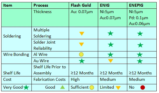
Advantages of ENEPIG over ENIG and Flash Gold
- Compared with other surface treatment methods, ENEPIG has the advantages of stable durability, excellent solder resistance, good compatibility, high coating flatness, and suitable for high-density pads, so it can be applied to more precise PCBs. The welding performance is also better.
- Intel first proposed ENEPIG, and now many BGA boards are used in gold bonding wire on one side, and soldering on the other.
- The thickness requirements of the gold plating layer on both sides are different. Bonding requires a thicker gold layer, about 0.3 microns or more, while solder only needs about 0.05 microns.
- The bonding is good if the gold layer is thicker, but the solder strength needs to be improved. If the gold layer is thinner, the soldering is OK, but the bonding is not good. Therefore, the previous process was covered with dry film, and gold plating with different specifications was done twice to meet the requirements.
- Now, ENEPIG with the same thickness specifications on both sides can meet the requirements of bonding and soldering. The current palladium and gold film thickness specifications are about 0.08 microns above, which can meet the requirements of bonding and soldering.
- More and more companies are widely using ENEPIG on PCB boards, including Microsoft, Apple, Intel, etc.
PCB Certification
Why Choose King Sun’s ENEPIG Technology?
ENEPIG is an advanced surface treatment option. As you know, it can meet the requirements of high-end electronic products. It is widely used in the manufacturing of high-density circuit boards.
In the field of ENEPIG technology application, King Sun has excellent technical strength and professional services. We ensure that we provide customers with first-class ENEPIG surface treatment solutions.
We manufacture 8 million PCBs annually, achieving an impressive customer satisfaction rate of 98%. Ensuring the lowest charges and fastest delivery in China, we are committed to providing swift and cost-effective services to our valued clients.