What is blind and buried via in PCB?

Blind and buried vias technology emerges in the requirement of miniaturization and high integration of electronic products. It is in order to improve the circuit density of PCB boards.

Blind Via: Blind via is connected from the inner layer to the outer layer. It does not penetrate the entire board.

Buried Via: The buried via is connected between inner layers, which can not be seen from the surface of the PCB.

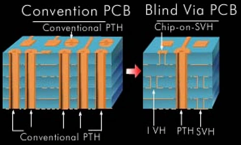
The process method of blind and buried vias

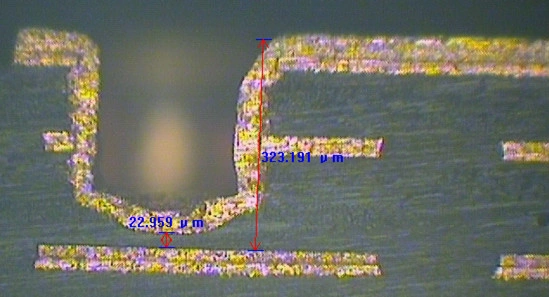
1. Depth Drilling Method

Use mechanical to drill the depth of the blind to achieve the connection between the inner layer and the outside layer. The drawback of this method is its low productivity, as only one piece can be machined at a time. Additionally, the processing is challenging, and reliability is compromised.

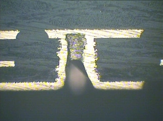
2. Sequential Laminating

Through repetitious pressing, I made out the buried vias, the blind vias, and the through hole successively. The weakness of this method is that it is not easy to control the expansion after repeatedly pressing; the processing is also long. This method can’t make cross-blind and buried vias.

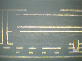
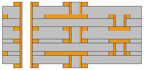
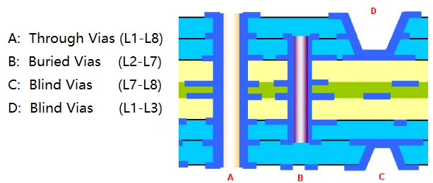
Blind via(L2-L4,L4-L8)
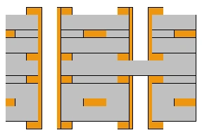
Blind vias(L1-L3)

3. HDI Build-Up

The method of laser drilling increases layer by layer for progressive lamination. Disadvantages: high-level equipment requirements, high plating ability, and high cost.

Process control in King Sun

  • We dedicated an FA team to calculate the pressure coefficient and reduce the pressure times that lead to quality problems.
  • X-ray shooting machine and OPE punching machine ensure accurate registration.
  • High-precision CNC drilling machine to ensure drilling accuracy
  • The blind and buried vias are made by plugging resin process, reducing the blasting hole without copper plate and risk.
  • CCD automatic parallel light exposure machine for small trace and highly accurate registration.

Blind and buried vias fabrication Capability

  1. Layer: Max. 20 Layer
  2. Min via size: 0.1mm for laser drilling, 0.15mm for traditional drilling
  3. Aspect ratio: < 12:1 for traditional drilling, >0.75:1 for laser drilling

Design suggestion of blind and buried vias

1. The Production Difficulty and Cost

The HDI laser blind and buried vias PCB is higher than the multiple lamination blind vias PCB, so try to avoid the design of cross-buried blind vias.

HDL laser drilling

Traditional blind vias

2. The connection of the metalized hole and circuit

Design ring width = minimum finish ring width + hole tolerance + etch tolerance.

Pad diameter = drill diameter +2 x minimum finish ring width + hole tolerance + etch tolerance.

Minimum finish ring width: 0.025mm.

Hole tolerance: +/-0.075mm.

Etch tolerance: +/-0.025mm.

When spacing is allowed, a teardrop pad is often used to ensure the safety connection between pads and wires.

3. Connection of Metallized Hole and Copper Area

A. Direct connection

B. Thermal pad connection (for reducing heat dissipation, making heat is concentrated on the solder)

Slit width: >=0.125mm.

The ring width is the same as the above requirement.

Inside diameter= drill diameter + 2x ring width.

4. Isolation of Hole and Line

The distance between hole to line and pad >=0.25mm.

The isolated pad diameter >= drill diameter+ 0.6mm.

Pay attention to the distance between the isolated pads when placing inner isolated pads.

Examples of common design errors:

5. Design points of Blank Area

Do not leave a large blank area without copper on the inner layer; it’s easy to warp, and copper foil wrinkles when laminate is pressed as the internal stress of the board is uneven. The outer layer should be as even as possible; do not leave a large blank area without copper; it can be filled with a nonfunctional square pad. Otherwise, plating, PTH and copper thickness will be uneven.

Fabrication Process Suggestion of Blind and Buried Vias

  • The best is a symmetrical structure to prevent the expansion caused by inconsistent PCB in serious warpage.
  • Use a core thickness as much as possible.
  • The inner layer tries to use the same type of copper thickness and the same copper thickness on both sides of each core.
  • Try to use the standard specification material of core and prepreg.
  • The better-buried vias diameter is 0.3mm~0.5mm; too large or too small is not conducive to plugging resin.
  • The minimum ring is 0.15mm for buried and blind vias. The minimum ring is 0.10mm for laser blind vias.