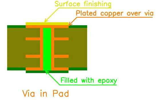
Via in PAD(VIP) PCB
What Is Via in Pad?
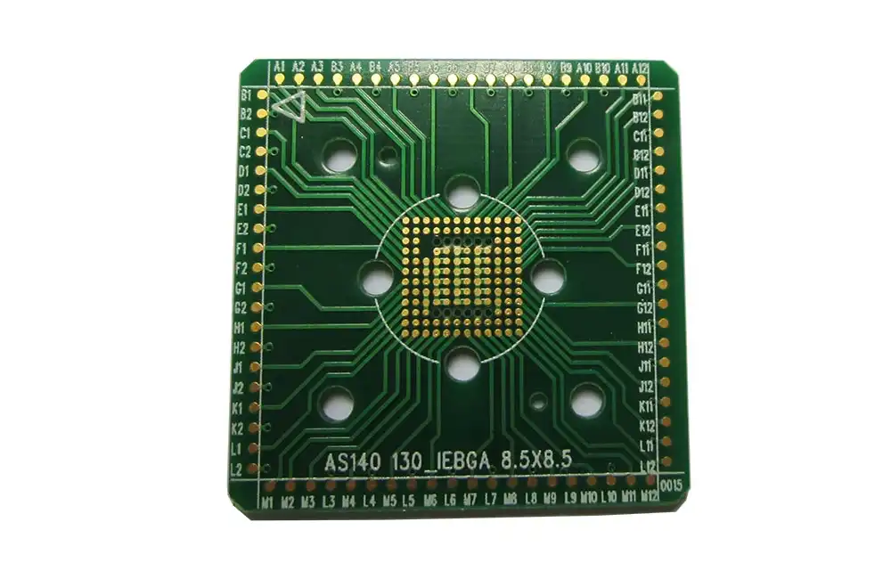
In PCB design, via in Pad (VIP) technology is commonly employed in compact PCBs with limited space for BGA.
There are three main types of Pad in Via. This includes through-hole vias, blind vias, and buried vias. They are used for circuit connections at different levels and provide design flexibility.
The via in pad process allows vias to be plated and hidden beneath BGA pads.
It required the PCB manufacturer to plug the vias with epoxy and then plate copper over it, making it virtually invisible.
The advantages and disadvantages of via in pad
When deciding whether to use filled via in pad technology, it is necessary to consider the advantages and disadvantages of this method.
PCB designers should accurately evaluate the project based on the actual situation to determine whether to use the technology.
The advantages of via in pad:
- Via in Pad can improve trace routing.
- Via in PAD can help thermal dissipate.
- Via in the pad can help reduce inductance in high-frequency boards.
- Via in pad can provide a flat surface for components.
However, there are some disadvantages:
- The price is high compared to normal PCB, a complex manufacturing process.
- Risk solder off of the BGA pad if you get low quality.
Via in pad Technical Principle
Plug the inner layer hole with resin and press it together. This technique balances the contradiction between the thickness control of the bonded dielectric layer and the inner hole-filling design.
- If the inner hole is not filled with resin, the board will explode when the heat shock occurs, and the scrap will be scrapped directly;
- If you do not use resin plugging, you need multi-sheet PP pressing to meet adhesive demand, but this way, the dielectric layer thickness between the layers will increase because the PP is too thick.
When should I use via in pad?
The via in pad plugging resin is widely used in HDI products to meet the design requirements of thin dielectric layers.
For the design of buried and blind holes in the inner layer. We often also need to increase the inner resin filling process because the middle medium design combined partial thin.
In certain scenarios, such as products with blind hole thickness exceeding 0.5mm, the conventional adhesive press may not be sufficient to fill the hole. In such cases, resin plugging is also needed to fill the vias to avoid blind holes without copper problems.
This process addresses design challenges related to thickness. Playing a crucial role in advanced PCB manufacturing, particularly for HDI applications, it significantly boosts the overall reliability and functionality of the printed circuit boards.
Produce process
Laminate Shear—>Drilling—>P.T.H.—>Panel Plating—>Resin Plugging—>Polishing—> PTH Drilling>P.T.H.—> Panel Plating—>Outer Layer Image—>Pattern Plating—>Etching—>S/M coating—>Surface Finishing—>Routing—>Test—>Backpacking&Shipping
Prevention and improvement measures for the problem of via in pad
- Use the appropriate ink and control the storage conditions and shelf-life of ink.
- Standard inspection procedure to avoid voids in pad holes. Even through excellent technology and good conditions to improve the yield of plugging, a 1/10000 change can also lead to scrap, sometimes just because only a void leads to scrap. This can only be done by checking for the location of the void hole and doing repairs. Of course, checking the plugging resin hole problem has always been discussed, but there seems to be no good equipment to solve this problem.
- The choice of the proper resin, especially the choice of the material Tg and the expansion coefficient, the proper production process, and the appropriate removal parameters, can avoid the problem of the pad separating from the resin after heating.
- For the problem of delamination between resin and copper, we found that the thickness of the copper on the hole surface is greater than 15um, and the problem can be greatly improved.