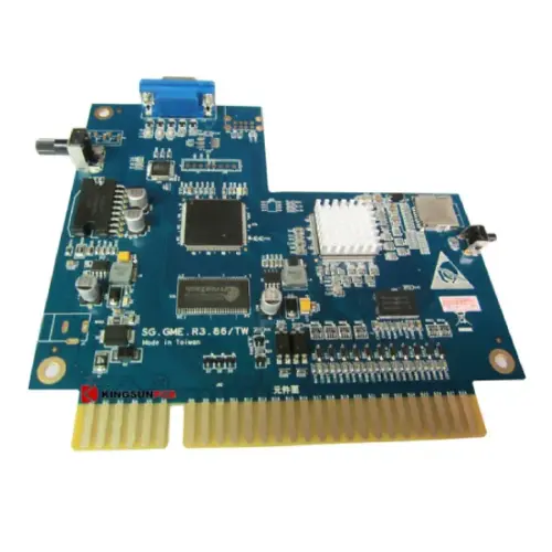
The Second Step Is PCB Board Manufacturing
The following are the main production procedures of conventional multilayer boards.
Material Cutting:
Cutting material is the large area (48in * 42in) of raw material that is cut into the working panel board that PCB manufacturers need.
Inner Layer:
The inner layer of the circuit uses positive imaging technology. After developing, etching, and de-filming processes, complete the production of the inner layer of the line.
Black Oxide:
Black Oxide is made before lamination. The main role is to roughen the copper surface and increase the surface contact area with the resin to ensure lamination quality.
Lamination:
Stack up the inner core and prepreg to press into a multilayer board through a vacuum pressure machine. And make the tooling holes for the next process.
Drilling: A CNC drilling machine dries holes for circuit connections between layers.
Electroless Copper:
Electroless copper is chemically deposited, copper. The method deposits a thin copper layer in the non-conductive substrate so that the through-holes are metalized. Then, the plating method thickens the hole's copper thickness to achieve the design purpose.
Copper Plating:
Copper plating is a method of electroplating to increase the thickness of through-holes and circuit surfaces.
Outer layer:
Transfer the outer pattern onto the copper-clad plate and etch the useless copper.
Solder Resist Character:
Printing a layer of insulated solder mask ink on the outer layer surface. Some PCBs also need to be printed symbols on the solder mask layer.
Surface treatment: Common PCB surface treatments include HASL, OSP, Immersion Gold, ENEPIG, Immersion Silver, Immersion Tin, and Gold finger plating.
Electrical Test:
All the PCBs must be pen/short tested before outgoing, including an electrical test and flying probe test. Electrical test for PCB mass production and flying probe test for samples as it's fast turn round.
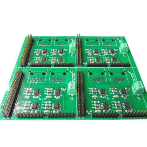
-gallery-770x578-1-500x500.jpg)
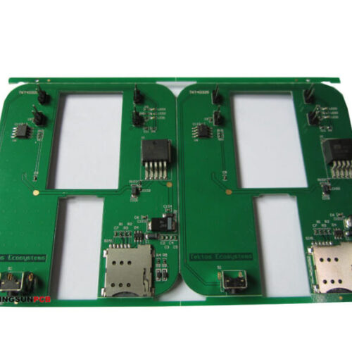
-gallery-770x578-1-500x500.jpg)