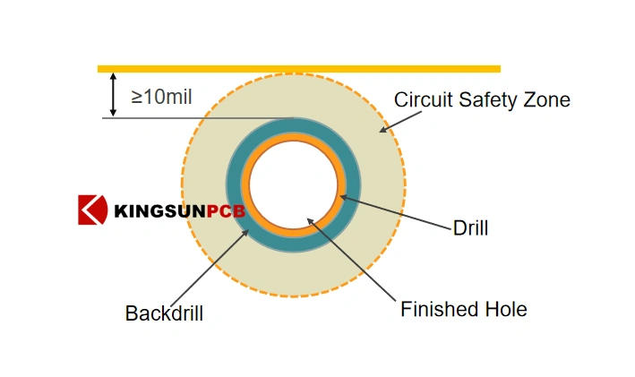
PCB trace to backdrill via spacing
The distance from the PCB trace to the edge of the back drilling hole is ≥10mil.
Back drilling, also known as controlled-depth drilling or back drilling, is used in printed circuit board (PCB) manufacturing.
Backdrill is a technology used in PCB design to carry high-fidelity signals faster. It’s commonly used in the semiconductor industry. This will minimize signal stubs.
Stubs are the source of impedance discontinuities and signal reflections, which become more critical as data rates increase. It is the preferred method in High-Speed signal designs.
By removing the excess copper from the non-connected layers, back drilling helps to eliminate signal reflections and impedance discontinuities that can degrade the performance of high-frequency signals.
This is particularly important in applications like high-speed data transmission, telecommunications, and RF circuitry. It helps to maintain signal integrity, reduce EMI, and ensure the smooth operation of electronic devices.
First, the elements of high-speed interconnection links:
The below figure shows a typical high-speed signal interconnect link:
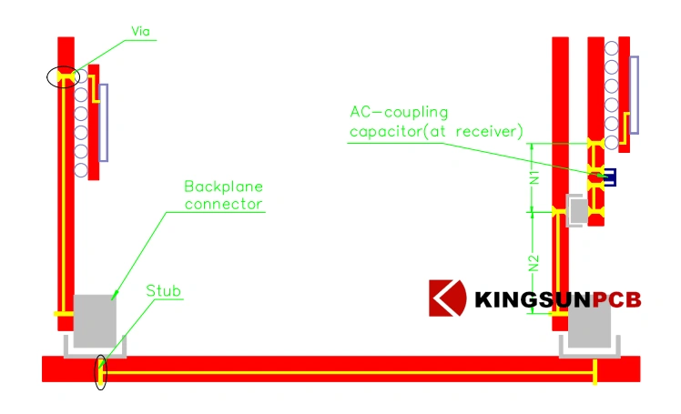
The high-speed signal interconnection links are relatively complicated. Usually, there will be an impedance mismatch problem at the different components’ connection points, resulting in signal emission.
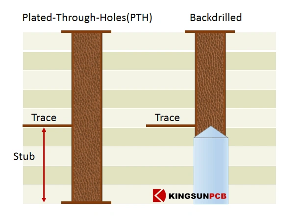
The PCB vias are usually designed as through holes (from the top surface layer to the bottom layer). If the PCB trace connected to the via is closer to the TOP layer, a “Stub” bifurcation will occur at the via hole. This can cause signal reflection and affect signal quality. This effect has a greater impact on higher-speed signals.
Therefore, it is necessary to find a way to remove the stub of the PCB through a hole. Back drilling is such a PCB processing technology.
The purpose of a back drill is to drill through a hole that does not have any connection or transmission to avoid reflection, scattering, and delay of high-speed signal transmission.
It is shown that the main factors that affect the signal integrity of the signal systems are that vias have a great influence on the signal integrity except for design, board material, transmission line, connector, chip package, and so on.
When the drill bit is drilled, the drill tip touches the copper foil of the substrate board, generates a micro-current to sense the height of the board surface, and then drills down according to the set drilling depth. It will stop when reaching the drilling depth.
The back drilling technology uses the depth-controlled drilling method to drill out the stub hole wall of the connector via hole or the signal via hole by secondary drilling.
As shown in the figure below, after the through-hole is formed, remove the redundant stub of the PCB through-hole by secondary drilling from the “back.” The process tolerance level ensures that “the remaining stub length is as small as possible” based on “not destroying the connection between the PCB hole and the wiring,” that is, the so-called “deep-controlled drilling.”
The figure above is a cross-sectional schematic diagram of the through-hole Back Drill. The left is a normal signal through-hole. On the right is a schematic diagram of the through hole after Back drilling, which means drilling from the Bottom layer to the signal layer where the trace is located.
Back drilling technology can remove the parasitic capacitance effect caused by the hole wall stub. Ensure that the impedance via the hole in the channel link is consistent with the trace, reduces signal reflection, and improves signal quality.
Backdrill is currently the most cost-effective technology for improving channel transmission performance. Using back drilling technology will increase the cost of PCB manufacturing to a certain extent.
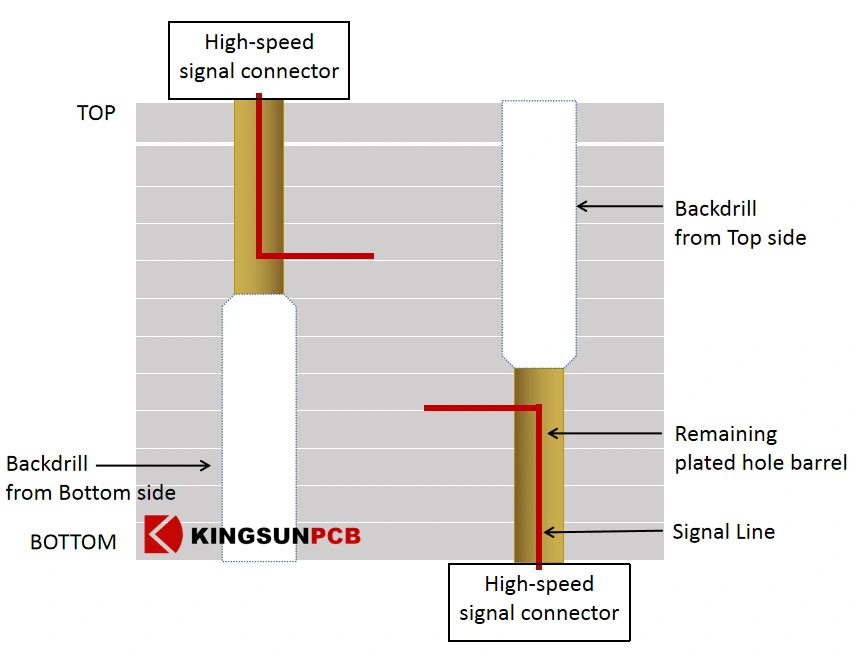
There are two types of back drilling: single-sided back drilling and double-sided back drilling.
Single sided drilling can be divided into back-drilling from the TOP side or back-drilling from the BOTTOM side. The PIN holes of the connector plug-in pins can only be back-drilled from the side opposite to the side where the connector is located.
When high-speed signal connectors are arranged on both the TOP and BOTTOM sides of the PCB, double-sided back drilling is required, as shown in the figure below.
Regarding back drilling depth control accuracy, the current capability can reach ±6mil. To improve reliability, it is better to keep a certain redundancy in the design, and it is recommended to meet the following design requirements.
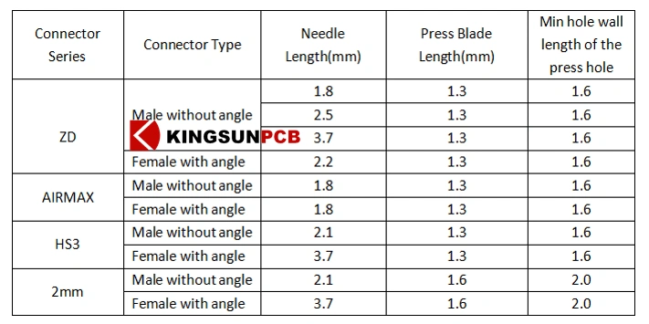
“Remaining hole wall length” of the PCB hole of the press-fit connector.
Design requirements: L≥L1+12mil.
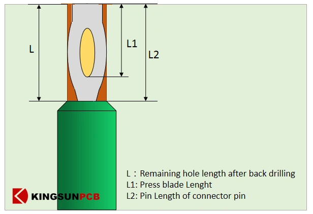
According to the above relationship, the minimum remaining hole wall requirements for different connectors via holes can be obtained, see Table 1 for details.
It should be noted that because the tolerance of the length L1 of the Press blade Length of the 2mm connector is slightly larger, it is slightly relaxed when determining the length L.
Keeping at least an 8mil stub for back drilling depth control is recommended. When designing the layer stack-up, we need to consider the prepreg thickness to avoid the wires being drilled and broken.
The back drilling depth control is recommended to be between two layers, and the thickness between the two layers is required to be ≥ 12mil.
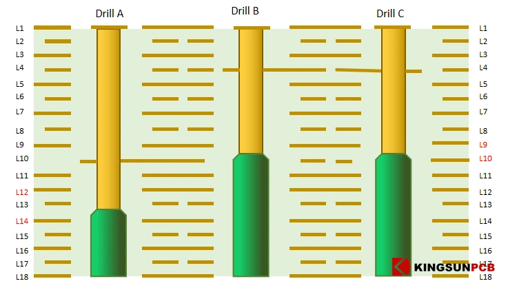
For example:
Back drill A:
When the adjacent two layers (such as L12 and L13, L13 and L14) do not meet the requirement ≥12mil, And when the distance between L12 and L14 is ≥12mil, The recommended back drilling depth is between L12 and L14.
Back drill B and back drill C:
When L9 and L10 ≥12mil, it is recommended that the back drilling depth be controlled between L9 and L10.
The distance from the PCB trace to the edge of the back drilling hole is ≥10mil.
Back drilling diameter (D) = drilling diameter (d) + 10mil
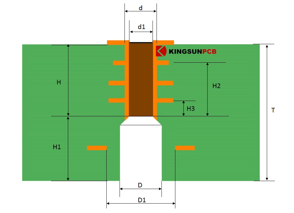
T: PCB thickness
d1: Finished hole diameter
d: Drill diameter
D: Backdrill diameter
D1: The distance between trace to backdrill
H: The remain hole length after back drilling
H1: The depth of back drill
H2, H3: The Stub length of signal trace
It is recommended that the distance between the back drilling hole and the inner layer graphics is ≥0.25mm and that the distance from the outer layer graphics is recommended to be ≥0.3mm.
The distance from backdrill hole to backdrill hole is ≥0.25mm.
No copper ring remaining after via pad back drilling
In order to recommend the back-drilled pads are designed according to the requirements as follows:
Pad on back drilling surface ≤ back drilling diameter
The inner pad is recommended to be designed as a padless process.
The surface treatment process of the back drill PCB requires OSP or chemical immersion tin/gold, and HASL is disabled.
The non-functional pads on the inner layer of the PCB are designed to be padless.
Add text on Smartdrill layer:
NO FUNCTIONAL PADS ON INTERNAL SIGNAL LAYERS MUST BE REMOVED.
Tips: The back-drilled surface of the back-drilled hole cannot be used for ICT testing at the same time.
In the PCB manufacturing process, back drilling is 2nd drill operation that removes the unused plating in vias from a certain side to a certain depth.
The major fabrication points of backdrilling:
Use a new drill tool to reduce chip load.
Check the fabrication capability of the depth of backdrilling.
Control precision of drilling.
Common understanding: Signals with a rate of ≥5Gbps need to consider adding a Backdrill design.
Of course, the design of high-speed interconnection links is a systematic project. If the chip drive capability is strong enough, or the system interconnection link is not long, the signal quality may pass without back drill design. Therefore, the most reliable method is to determine whether a back drill is needed through system interconnection link simulation.