Castellation PCB Technology
What is Castellated PCB?
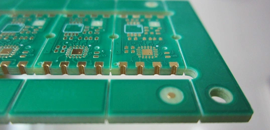
Castellated PCB is PCB metalized holes cut in half on the edge. It can directly weld the hole’s edge to the main board, saving connectors and space. Lots of modules are designed with castellated holes PCB.
What are the main types of castellated holes?
The castellated PCB design mainly focuses on communication modules such as Bluetooth and NBloT modules. It usually appears in signal circuit boards. Below are the main types of castellated holes.
Semi-hole
Bigger than semi-hole
Hole tangent to PCB edge
Advantages of castellated holes
- Castellated PCB is small.
- Easy to solder, There is a whole row of metalized half-holes on the side of the PCB. The daughter board and motherboard are welded together through the metalized half-holes.
Disadvantages of castellated holes
- It has a Jagged shape after the PCB board is separated. It is easy to block the case and sometimes needs to be cut with scissors. Therefore, it is necessary to reserve space in the PCB design process, generally shrinking the board.
- Increase cost. The minimum castellated hole is 0.6mm, and PCB technology is complex, so the PCB cost is higher than that of regular PCBs.
Castellated Hole Requirements
Size: It is recommended to use the largest possible dimension
Surface treatment: It depends on the end use of the board, but ENIG is recommended.
Tooling holes: This depends on the design; however, it is well known that the lower the holes, the more complex the PCB assembly process.
How to Design the castellated hole?
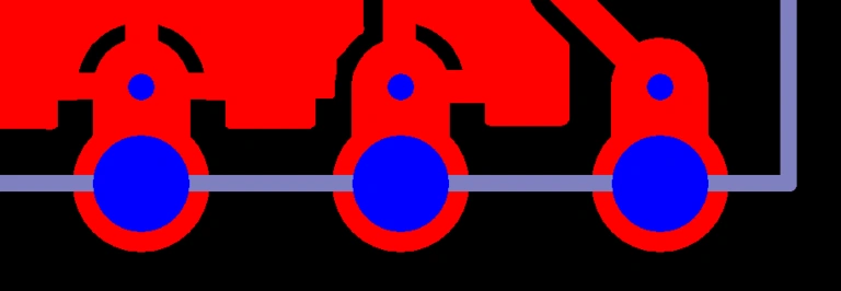
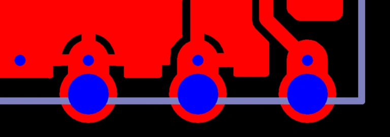
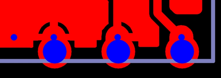
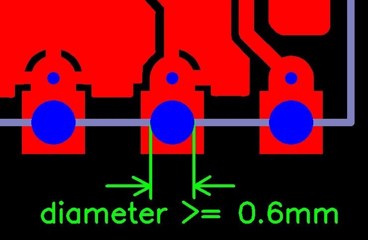
Castellated hole size diameter ≥ 0.6MM
Castellated hole size diameter ≥ 0.6MM
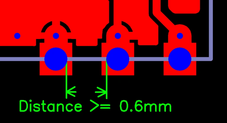
The distance of hole edge to hole edge ≥ 0.6MM
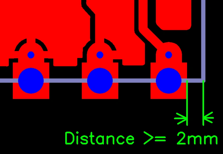
The distance is between PCB edge to hole edge ≥ 2.0mm
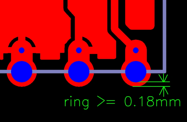
The castellated hole ring≥ 0.18mm
Castellation PCB Process
Castellated holes are the process of cutting half of the metalized hole. It seems very simple, as long as the final milling shape is done on the conventional processing plate, but it is not.
- Double V-shaped cutting tool for processing castellated holes.
- Adds guide holes on the edge of holes of second drilling, removes the copper skin in advance, reduces burrs, and uses routing cut instead of drills to optimize the drop speed.
- Immersion of copper to plate the working panel so that a layer of copper is electroplated on the hole wall of the round hole on the edge of the board.
- In outer layer circuit production, the working panel is pasted dry film, exposed, and developed in sequence, and then second copper-plated and tin-plated on the working panel. Thick the copper layer on the castellated holes of the edge PCB board and protect the copper layer with a tin layer.
- Castellation PCB cut the round hole on the edge of the board in half to form Castellation holes.
- In the step of removing the film, remove the anti-electroplating film.
- Etching the working panel, and removing the exposed copper after the film peeled.
- Stripping the Tin layer, so that the tin on the half-hole wall can be removed, and the copper layer on the half-hole wall is exposed.
- After milling, use red tape to stick the unit boards together and remove the burrs through alkaline etching lines.
- After secondary copper plating and tin plating on the working panel, the round hole on the edge of the board is cut in half to form castellated holes.
- The castellated holes can be prevented from peeling off when cutting, Since the copper layer of the hole wall is covered with a tin layer, and the copper layer of the hole wall is completely connected with the outer layer of copper.
- After castellated hole milling is completed, the film is removed and then etched, so that the copper surface will not be oxidized, effectively avoiding the residual copper or even short circuit, and improving the yield rate of the metalized castellation PCB circuit board.
What are the difficulties in processing Castellated PCB?
- The castellated holes PCB is always having problems in the process, like back copper skin on the hole wall, residual burrs, and misalignment after milling.
- PCB castellated edges, it’s easy to lead short circuits due to the space between holes being very small.
- The general castellated edges PCB process methods include CNC milling machine, mechanical punching, V scoring CUT, etc.
- Different processing methods will inevitably lead to residual copper wires and burrs on the cross-section of the remaining PTH holes when removing the unuseful copper. Even worse, the copper skin on the entire hole wall will be peeled off.
- When making castellated holes, the size is a deviation on the left and right in the same unit of the remaining half holes as PCB expansion and shrinkage, drilling hole position accuracy, and milling accuracy. It easily leads to soldering trouble.