OSP PCB Technology
What is OSP PCB?
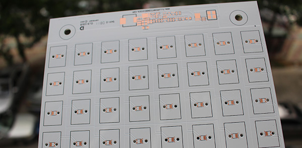
OSP is a process for the surface treatment of printed circuit board (PCB) copper foil in accordance with the requirements of RoHS. OSP is the abbreviation of Organic Solderability Preservatives. It is also called “organic solder protection film”. It is also called “copper protecting agent”. It is also called Preflux.
OSP is chemically grown a layer of organic film on the surface of cleaning bare copper. The film has oxidation resistance, thermal shock resistance, moisture resistance, for protecting the surface of copper in the normal environment no longer continuing to rust (oxidation or curing), but this protective film must be very easy and rapidly cleared in follow-up welding heat, so that clean exposed copper and molten solder immediately combined into a solid solder joint in a very short period of time.
Printed circuit boards are more and more high precision, thin, multi-layered, small holes along with electronic products are light and thin, short, small developing, especially the rapid development of SMT, the hot air leveling has not adapted that high density boards. At the same time, hot air leveling using Sn-Pb solder does not comply with environmental requirements. With the formal implementation of the EU RoHS directive on July 1, 2006, the industry is urgently seeking lead-free alternative to PCB surface treatment, the most common are organic solder protection (OSP), electroless nickel immersion gold (ENIG), immersion silver and immersion tin.
The following figure shows a few common PCB surface treatment methods, hot air leveling (Sn-Pb, HASL), immersion silver, immersion tin, OSP, electroless nickel plating gold (ENIG) performance comparison, of which the latter 4 for lead-free process. It can be seen that OSP is more and more popular in the industry because of its simple process and low cost.
| Physical Properties | HASL | Immersion Sliver | Immersion Tin | OSP | ENIG |
| Storage Life | 12 months | 6 months | 6 months | 6 months | 12 months |
| Experience reflow times | 4 | 5 | 5 | 4 | 4 |
| Cost | Medium | Medium | Medium | Low | High |
| Process complexity | High | Medium | Medium | Low | High |
| Process temperature | 240°C | 50°C | 70°C | 40°C | 80°C |
| Thickness range(um) | 1-25 | 0.05-0.2 | 0.8-1.2 | 0.2-0.5 | Au:0.05-0.2,Ni 3-5 |
| Flux compatibility | Good | good | good | good | good |
Technological process
Degreasing—>Water cleaning—>Microetch—>Water cleaning—>pickling—> DI water cleaning—>Formed film and drying—>DI water cleaning—>Drying
1. Degreasing
The effect of oil removal directly affects the quality of film formation. The film thickness is uneven when the oil is not clear. On the one hand, the concentration can be controlled within the range of the process by analyzing the solution. On the other hand, often check whether the effect of degreasing is good, if the oil removal effect is not good, it should be promptly replaced with oil removal.
2. Microetch
The purpose of etching is to form a roughened copper surface to facilitate film formation. The thickness of the etching directly influences the rate of film formation. Therefore, it is very important to maintain a stable thickness of the film to maintain the thickness of the etched film. Generally, it is appropriate to control the etching thickness at 1.0-1.5um. The micro corrosion rate can be determined before each production, and the etching time is determined according to the micro etching rate.
3. Film formation
DI water is best used for washing before film formation, so as to prevent contamination of the film forming fluid. After the film is washed, it is best to use DI water, and pH value should be controlled between 4.0-7.0, in case the film is contaminated and damaged. The key to the OSP process is to control the thickness of the oxide film. The film is too thin, heat shock resistance ability, in reflow soldering, film resistance to high temperature (190-200 ~ C), and ultimately affect the welding performance in electronic assembly line. Film is not very good in the flux of dissolved, welding performance. The average control film thickness is between 0.2-0.5um.
Weakness
- OSP, of course, has its drawbacks. For example, there are many kinds of practical formulas and different performances. That is to say, the certification and selection of suppliers should be done well enough.
- The disadvantage of the OSP process is that the resulting protective films are extremely thin and easy to scratch (or abrade) and must be carefully operated and operational amplifiers. At the same time, after many times of high temperature welding process, the OSP film (the OSP film on the non welded connecting plate) will change color or crack, which will affect weldability and reliability.
Packaging and storage
OSP is thin organic coating on the surface of PCB, if a long time exposure to high temperature and high humidity environment, the occurrence of PCB surface oxidation, weldability variation, after reflow soldering process, organic coating on PCB surface will be thinner, resulting in PCB easily oxidized copper foil. Therefore, the preservation methods and use of OSP PCB and SMT semi-finished products shall comply with the following principles:
- OSP PCB shall be packed in vacuum with a desiccant and humidity display card attached. Transport and storage of PCB with OSP shall be made using isolation paper to prevent friction from damaging the OSP surface.
- Should not be exposed to direct sunlight environment, maintain a good storage environment, relative humidity: 30~70%, temperature: 15~30 C, storage period is less than 6 months.
- Opened on the SMT site, must check the humidity indicator card, and on-line 12 hours, never once open a lot of the package. If not finished, or is it a device to solve the problem for a long time, it is prone to problems. After printing the furnace as soon as possible not to stay, because there is a very strong flux solder paste on the OSP coating corrosion. Maintain a good workshop environment: relative humidity 40~60%, temperature: 22~27 degrees celsius. In the process of production, it is necessary to avoid touching the PCB surface directly with hands, so as to prevent the surface from being oxidized by sweat pollution.
- The second side SMT assembly must be completed within 24 hours after the completion of first side SMT assembly.
- Finished the DIP in as short a time as possible (the longest 36 hours) after completing the SMT.
- OSP PCB can’t be baking. High temperature baking easily deteriorates color of OSP. If bare board exceeds the storage life, it can be returned to OSP manufacturer for rework.