The Second Step Is PCB Board Manufacturing
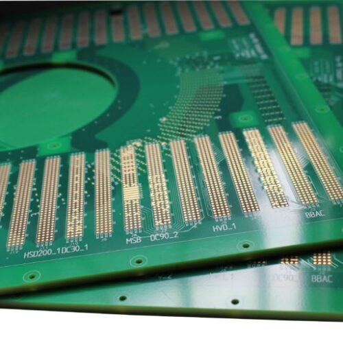
The following are the main production procedures of conventional multilayer boards.
Material Cutting: Cutting material is the large area (48in * 42in) of raw material that is cut into the working panel board that PCB manufacturers need.
Inner Layer: The inner layer of the circuit uses positive imaging technology, After developing, etching, and de-filming processes, complete the production of the inner layer of the line.
Black Oxide: Black Oxide is made before lamination. The main role is to roughen the copper surface and increase the surface contact area with the resin to ensure the quality of lamination.
Lamination: Stack up the inner core and prepreg to press into multilayer board through vacuum pressure machine. And make the tooling holes for the next process.
Drilling: Using CNC drilling machine, through holes are drilled for circuit connections between layers.
Electroless Copper: Electroless copper is chemically deposited, copper. The method deposits a thin copper layer in the non-conductive substrate so that the through-holes are metallization. Then use the plating method to thicken the hole’s copper thickness to achieve the design purpose.
Copper Plating: Copper plating is a method of electroplating to increase the thickness of through-holes and circuit surfaces.
Outer layer: Transfer the outer pattern onto the copper-clad plate and etch the useless copper.
Solder Resist Character: Printing a layer of insulated solder mask ink on the outer layer surface. Some PCBs also need to be printed symbols on the solder mask layer.
Surface treatment: Common PCB surface treatments include HASL, OSP, Immersion Gold, ENEPIG, Immersion Silver, Immersion Tin, and Gold finger plating.
Electrical Test: All the PCBs must be pen/short tested before outgoing, the test included electrical test and flying probe test. Electrical test for PCB mass production and flying probe test for samples as it’s fast turn round.

