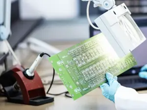
How are PCBs manufactured? It is one of the exciting questions PCB hobbyists ask. The process of manufacturing PCB boards is lengthy and complicated. Its manufacturing process involves multiple steps. The circuit board can cause performance issues if we do not follow the correct method.
PCB development requires expertise from beginning to end. It mainly depends on innovative production methods and expertise in electronic systems.
As one of the leading PCB manufacturers, we have been operating on the market for several years. The production process and execution of our customer’s orders follow international standards. With us, you can implement your own PCB design.
There are three main types of PCBs
- Single-sided printed circuit boards
- Double-sided printed circuit boards
- Multilayered printed circuit boards
There are functional and structural distinctions between the above-printed circuit boards. As a result, their PCB manufacturing techniques may also have slight differences. Click here to see more standard PCB stackups.
A comprehensive guide to the PCB design and manufacturing process. Every step from design to finished product is covered, such as chemical etching, lamination, drilling and quality control.
Remember that the greater the number of sides a PCB has, the more complex its production method is. Therefore, to correctly understand how to create PCBs, choosing the type of PCB you want is essential.
What are the parts of a PCB?
A PCB has four main components:
The Substrate
The substrate material typically consists of fiberglass. The first part is crucial. Fiberglass provides the PCB core strength and helps it withstand breakage.
Layer of Copper
This layer includes a copper foil. It depends on the type of PCB board. The purpose of the copper remains the same, regardless of the method used. It is used to carry electrical messages to and from the PCB.
Solder Mask
The solder mask is the third component of the PCB. It is a polymer layer that protects copper from its surrounding environment. The solder mask acts as the “skin” of the PCB.
Silkscreen
The silkscreen is the final part of the PCB board. The silkscreen displays part numbers, logos, and switch settings.
What is the PCB Manufacturing Process?
The PCB fabrication method requires an innovative approach. The aim is to make a fully operational PCB board. After the production of the initial layer of the PCB board, the manufacturing processes change.
Because of design modifications, certain PCBs may require more than fifteen production steps. As the PCB board manufacturing process requires more steps, printed circuit boards become more complex. Learn the PCB manufacturing process in more detail.
Missing steps or simplifying the method can harm the PCB board’s performance. However, the PCBs should work smoothly after the final production.
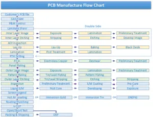
Steps Involved in the PCB Manufacturing Process
The PCB design and manufacturing process includes the following steps.
Step 1: PCB design and DFM
Step 2: Base Substrate Chosen
Step 3: Substrate Cutting
Step 4: Inner Layer Pattern Printing
Step 5: Exposure to UV Light
Step 6: Copper Removal
Step 7: Inner Layer AOI Inspection
Step 8: Lamination and Pressing
Step 9: Drilling and Plating
Step 10: Outer Layer Imaging
Step 11: Plating and Etching
Step 12: Solder Mask Application
Step 13: Silkscreening, Surface Finish, and Testing
PCB Design and DFM
finalDefining a PCB’s functionality before starting with the PCB board’s manufacture. A PCB’s design is curated according to its functions. PCB designers create a design plan using many software programs. The steps still need to be completed. The designer examines if there are any defects.
After the examination, the production team receives the PCB design from the design department. It is used to make PCBs. The PCB fabrication team also performs DFM testing at this stage.
Base Substrate Chosen
The next stage starts after engineers thoroughly review the PCB design to ensure no mistakes or missing parts.
The substrate plays a crucial role in holding various components in PCBs. Consequently, glass fiber and epoxy resin, both insulators, are the preferred substrates. The primary PCB material is copper on both sides.
The most common type is glass-reinforced epoxy, commonly referred to as FR-4. In addition, materials with metal, polyimide, and ceramic cores are used.
Substrate Cutting
After selecting the base material, it’s time to start manufacturing the PCB board. The base materials usually come in large sheets to reduce production and transportation costs. It allows PCB makers to produce PCBs of any size.
However, a vast sheet size of 41 by 47 inches is hard to make. Therefore, we must cut these large sheets into 18 by 24 inches or fewer parts. However, depending on the dimensions of the printed circuit boards, we can cut them into various ratios.
Inner Layer Pattern Printing
You must understand a few terms before beginning this phase. The laminate panel serves as the structure’s main foundation. Resist is a photo-sensitive film. Chemicals that react to UV light to form a hardened layer are called photo-reactive materials.
At this stage, the laminate is printed with the PCB design. With the help of registration holes, everything is again aligned when printing is finished.
It involves using a specialized “plotted printer” printer to print the PCB design. This method provides PCB manufacturers with a film showing every component of the PCB.
The film acts as a “negative” because the colors used to show the layers differ from those on the board.
Clear ink represents non-conductive areas, while black ink is used for copper lines and circuits on the interior layer. The colors used in the outermost layer are the same but placed separately. In other words, non-conductive zones are labeled with black ink, whereas conductive areas are marked with clear ink.
A multilayered PCB is made on separate films for each layer. The next step is to punch a registration hole to help in alignment through these PCB layers and films.
Exposure to UV Light
PCB manufacturers then use ultraviolet light to show the laminate and resist. The copper channel is visible on the hardened part of the resist. Printing requires the use of black ink.
An alkaline wash can help clear the photoresist from these areas. A technician checks the PCB board for defects once it has dried.
Removal of Excessive Copper
For the board to function correctly, excess copper needs to be removed. It must be coated before the process begins to protect the copper from the chemical that removes excess copper. We also refer to this as the process of “etching.” The material and size of PCBs define how long this phase takes.
Inner Layer AOI Inspection
After the PCB layers, PCB experts check the board for flaws using AOI devices. Be careful that a damaged PCB board can lead to electrical shorts or stop working. This step is crucial in the “How is a PCB manufactured: Step-by-Step Guide” series. We will move on to the next step if it passes the examination and has no defects.
Lamination and Pressing
A unique press table is needed for this kind of process. First, an epoxy layer is applied at the base of the basin. Afterward, there is a layer of copper foil and substrate. Before placing a press plate, more prepreg layers are set up.
The pressing operation is also done with the support of another machine. Pins pierced through them to secure the layers in place. The machine-applied pressure and the epoxy’s melting process help in the fusion of layers.
Drilling and Plating
Computer-guided drilling is needed to access the inner PCB layers following lamination. An X-ray machine tracks the drill locations to avoid failures. The next step is to carry out an additional copper-removal process. A PCB gets several chemical washes after drilling, fusing, and polishing.
Outer Layer Imaging
The technique requires applying photoresist in an approach similar to that mentioned earlier. The photoresist UV light exposure starts after using the photoresist to the outer layer.
We remove the extra photoresist first.
Plating and Etching
Another thin layer of copper applies to the panel, similar to step 9’s plating technique. A tiny tin guard is applied to the panel to prevent this copper layer from being wiped.
The etching follows. Your guess was correct! Unwanted copper gets removed using chemical solutions again. Under the tin guard, the copper remains secure. This step has completed all PCB connections.
Drilling Holes – PCB Circuits
We make base holes based on the prepared files for drilling in the forms.
The pieces are assembled into packages (2-6 pieces) depending on the thickness of the laminate used in production.
Our business profile also includes production based on FR4, CEM1, and FR2 materials:
- Insulating spacers
- Mounting plates,
- Load-bearing boards in the thickness range from 0.2 to 5 mm
Cleaning the Surface Before Applying PCB Layers
Before applying the print mosaic, clean the copper surface. The cleaning process is followed by rinsing and drying with hot air. The type and hardness of the brushes used are essential.
Applying a protective layer against etching
We apply a mosaic of screen printing onto the cleaned laminate surface.
These methods differ in time consumption and the precision of the security measures performed.
Copper Etching
An adequately hardened protective layer allows you to proceed to the following process, i.e., etching.
We apply the etching agent. It washes away the unprotected copper surface. The PCB boards move on a roller conveyor with adjustable speed.
After etching, the printed circuits come in a protective layer. Similarly, we clean them before applying a solder mask layer.
Applying A Layer of Solder Mask
Using screen printing, we apply a solder mask layer to the brushed laminate surface. Screen printing is a process that uses different mesh screens. The purpose is to achieve the desired resolution and paint thickness. We use UV and IR hardened in the following colors:
- Green matte and glossy
- Blue
- Red
- Black
- White
- White, non-yellowing (used in LED panels)
- Yellow
Application of Solder Mask
Can PCBs function properly without using a solder mask? Therefore, professionals move on to the next step after thoroughly washing each panel.
Here, they use the solder mask film to set the epoxy. The solder mask coating provides a PCB with its unique green color. Again, UV light is used to remove unneeded solder masks.
PCB with ENIG Surface Finish
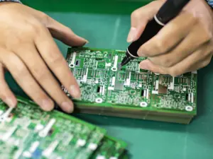
This last step effectively determines the manufacturing and functioning of PCBs. Silkscreening adds essential details to a PCB, such as manufacturer’s marks and business ID numbers. Therefore, PCBs receive the silkscreening process after the solder mask application. This approach commonly makes use of an inkjet printer. Additionally, there’s another session dedicated to coating and drying.
The solder gets a surface polish to boost its quality and bond. The most common surface finishes are:
Finally, a technician tests the PCB to ensure it meets the requirements and design. Technicians prepare the PCBs for installation after completing the machining and inspection processes.
Documentation Required for The Production of Printed Circuit Boards
Documentation necessary for PCB production:
All used PCB layers should be generated from the project in. gbr. cam format.
Source files from PCB design programs (optimal for the customer):
- Protel
- Eagle
- KiCad
- Rimu
- Express PCB
We send the PCB design for approval after making the mosaic in the PCB program.
Possessed PCB films
It consists of:
- 1200dpi positive and negative films
- Drilling and milling text file
- Screens for the printing layer- 120 mesh
- Sieves for the technological description layer – 120 mesh
Conclusion
Transforming a PCB design into a working board is complex. It goes through several complicated steps. But every step, no matter how small, is essential for building a reliable and functional PCB. For this purpose, hiring a professional PCB manufacturer is paramount.
The production of PCBs is preceded by proper verification of the technical documentation. Kingsun PCB precisely follows all essential steps in PCB manufacturing. We use modern software to prepare production files and test boards. Thanks to this all our products meet the quality requirements. Subsequently, our PCBs are free from any defects. To get a free PCB board quote and PCA services, contact the KingSun PCB team.