Introduction
Look at the board inside a small toy or motherboard on your computer. And think, what are these?
All these are examples of PWB or PCB. How do you define and compare them?
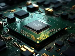
These are the Printed Wiring Boards (PWB) and Printed Circuit Boards (PCB). They are vital components in modern electronics. These support and connect several electronic components, systems, and products.
Keep reading, as this article will look at these two in detail.
You will learn the differences between PWB and PCB and what you should choose. You will also explore how these two terms are frequently used interchangeably.
What is a PWB?
Definition
You might be curious and want to know the meaning of PWB.
PWB is short for Printed Wiring Board. It serves as a basis for connecting electronic components.
Let’s look at its components and manufacturing procedure.
Components
A PWB board comprises conduction-enabling traces etched onto a non-conducting substrate.
Traces
The traces are usually thin copper strips. The non-conducting substrate is epoxy glass. This forms a conductive circuit. They allow for electrical connections between components.
Substrate
The substrate provides electrical insulation and mechanical support for the traces. Besides epoxy glass, other examples of substrates include phenolic paper, prepreg, and polyimide.
Through Holes or Vias
PWB also has through-holes or vias that help to mount electrical components.
A Printed Wiring Board serves as a physical platform for interconnected electrical components. These can be integrated circuits (ICs), capacitors, and resistors.
PWB is single-sided. Such a board is usually single-sided, meaning the traces are on one side of the substrate. This is a limitation of PWB design, restricting the circuit complexity of such a board. That’s why it’s more suitable for simpler devices and applications.
PWB Manufacturing Procedure
The manufacturing of PWB electronics involves many steps:
Preparation of Substrate
The first step is the substrate preparation. This step involves cutting the substrate to the required size and cleaning.
Further treatments like surface roughening are also done.
Creation of Pattern
The next step is about creating a pattern on the substrate. Several methods can do this.
One method is photolithography. It involves the application of photoresist (light-sensitive) material to the substrate. Then it’s exposed to UV light leading to the development of resist material. This creates the pattern.
Other methods for pattern creation include screen printing or direct imaging techniques. Screen printing applies the resist material in the needed pattern on the substrate. This can be done through a screen.
Direct imaging techniques usually use a laser to expose the resist material.
Etching
The next step in PWB electronics manufacturing is etching.
Using chemical etchants, the exposed parts of the substrate are etched away. An example of a chemical etchant used is ferric chloride. The conductive traces are left behind as a result.
The residual resist material is then removed. The result is the creation of the final circuit pattern.
Surface Finishing
In the next step, a surface finish is used. This prevents copper from oxidation and enhances the soldering capability during the component assembly.
Further processes
Further processes may include drilling holes and quality control inspections.
What is PCB Stand For?
Definition
What does PCB stand for?
PCB is short for Printed Circuit Board (also called PCB board). This term precisely describes a mainboard that supports and interconnects electronic components.
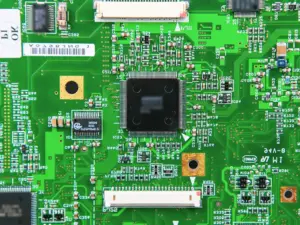
A PCB typically comprises several layers of conductive traces and materials for insulation. This allows for a more complex circuit design and adds more functions to the circuit.
PCBs are used widely for various applications like consumer electronics and aerospace systems.
Let’s look at its components and manufacturing method:
Components
A Printed Circuit Board is made of various components.
Substrate
The first is the substrate: the base gives electrical insulation and mechanical support for the traces.
The most popular substrate material is FR-4, which means flame-retardant fiberglass epoxy. By flame-retardant, we mean it will slow down the spread of fire. This material has excellent mechanical strength and electrical insulation.
Traces
Next are the traces on PCBs that are usually made of copper. This material has excellent electrical conductivity and low cost.
Vias or Small Holes
There are also vias or small holes on the board. These provide electrical connections between the layers of traces. They further act as mounting points for various electronic components.
Solder mask
The last component of a Printed Circuit Board is a solder mask. It’s a slim layer of insulating material applied to the PCB surface. During PCB assembly, it protects the traces from oxidation, short circuits, and impurities.
There are various solder mask substances like liquid photoimageable (LPI) solder masks.
PCB Manufacturing Procedure
Manufacturing of printed circuit boards (PCB) has several steps. View a step-by-step guide to the PCB manufacturing process.
- PCB Design
The first is the design of PCB via CAD (computer-aided design) software.
- Preparation of Substrate
The next step is substrate preparation. Here, the substrate undergoes cutting and cleaning; then, a thin copper foil layer is applied.
- Pattern Creation
The following procedure is pattern creation on the copper foil. This is done via several methods like photolithography and laser direct imaging (LDI).
In photolithography, a photosensitive resist material is applied to the foil. Then, UV light exposure is done. The development of resist material follows this to create the pattern.
- Etching
After pattern creation, the exposed regions of copper foil are etched away, leaving traces. Chemical etchants in this process are used in making the final circuit pattern.
- Drilling Holes
The next step is drilling the holes in the PCB. This aids in mounting and supporting the components.
- Plating
Plating is done next. It means a thin copper layer is placed onto the walls of the drilled holes. This can be done via methods like electroplating.
- Surface Finishing
The final step in Printed Circuit Board (PCB) manufacturing is surface finishing.
Here, a surface finish material like Hot Air Solder Leveling (HASL) is applied. It protects the traces from oxidation.
- Further Processes
There can be more processes like quality control inspections. This ensures the board is ready for component assembly.
PCBA vs PCB: An Overview
PCBA is short for Printed Circuit Board Assembly. It’s a PCB board with all required electronic components (like ICs) mounted and soldered.
PCBA aims to be a platform for the electronic components to work together.
PCB assembly is the process of assembling a PCB with all the components. Meanwhile, PCB is a board with traces and insulating material but no electronic components.
PWB vs PCB: A look at chief differences
The following are the chief differences between PWB and PCB:
| Printed Wiring Board (PWB) | Printed Circuit Board (PCB) |
| Usually single-sided | Is single-sided, double-sided, or multilayer |
| Favorable for simple electronic devices and applications | Favorable for complex circuitry, advanced and high-density components, and electronics |
| PWB is a less popularly used term | PCB is a more popularly used term |
| Manufacturing involves simple and cost-effective processes, e.g. photolithography. | Manufacturing involves more high-level and expensive techniques like laser direct imaging. |
| Typically has epoxy glass as the substrate | Typically has FR-4 as the substrate |
| PWB design must be according to simple industry standards | PCB design is according to strict standards like those set up by bodies like IPC |
| Also known as a bare board | It’s a part of printed circuit board assembly (PCBA) or printed wiring assembly (PWA) |
| Examples of applications include simple consumer electronics, power supplies, and auto electronics. | Used in smartphones, computers, healthcare devices, advanced auto electronics, etc |
PCB and PWB, how should I choose?
Like many, you may need clarification when choosing between these two boards. There are several factors you should keep in mind when choosing these two boards:
Complexity of Electronic Devices
You need an electronic device with complex circuitry, advanced functions, or high-density parts. Then, choose a Printed Circuit Board (PCB).
For high-performing electronic devices, you need a PCB. Examples of these devices include high-end computers and data servers.
PCB is preferred for devices with high component density in small spaces, e.g., smartphones.
Your need could be a simple and less complicated electronic device. In that case, you can select Printed Wiring Board as it can fulfill your needs. Some examples of using it include remote controls and small household appliances.
Budget
PCBs are usually more expensive to manufacture as compared to PWBs.
Your budget requirements may be lower. It’s wise to pick PWBs as you can manufacture them within a tight budget.
Otherwise, choose PCBs as they typically need a high budget to manufacture.
Production Time and Volume
You may need the boards produced in a shorter time. Then a Printed Wiring Board is preferred.
If you need low to medium production volume, then it’s also the obvious choice. Otherwise, Printed Circuit Boards are preferred to be selected.
Can you use PWB and PCB interchangeably?
You now know the differences between PWB and PCB.
But can you use PWB and PCB interchangeably? This question needs to be clarified because there is no official precise terminology.
Variations exist in these two terms across different geographic regions, industries, and periods.
Variations Across Geographic Regions
Today, in the USA, PCB is widely used. However, PWB has also been traditionally used interchangeably in the country.
In modern Japan, the term PWB has replaced PCB. This is to avoid confusion with polychlorinated biphenyls. It’s a poison that’s generally available there.
When the electronics industry was new in the 20th century, PCB was preferred in Japan.
Variations Across Industries
There are also variations in the terms across varying industries. For example, the electronics industry prefers PCB.
Meanwhile, the aerospace industry may incline toward PWB as it’s more linked to wiring technologies.
Variations Across Periods
Regarding time, Printed Wiring Board was an earlier term when the electronics industry was born. But Printed Circuit Board is a modern term and is more widely used today.
These terms have appeared in documents from different regions, periods, and industries.
What is the Future Development Trend of PWB and PCB?
Both PWB and PCB will continue to develop further. These changes will be as per market needs and innovations in technology.
The goal is to develop high-density, superior precision, multilayer, highly reliable, thin, and lightweight boards.
The future Printed Circuit Board technology will also achieve energy-saving and environmental goals. Thus, the manufacturing of future PCBs will be more environmentally friendly.
Both PWB and PCB will also grasp intelligence and undergo functions like self-repair.
Conclusion
You must have learned about Printed Wiring Boards and Printed Circuit Boards.
The continuing evolution of these two has led to remarkable growth in the electronics sector.
Printed Wiring Boards are suited for simple designs and circuits with low component density. Printed Circuit Boards allow complex design and fitting circuits with high component density.
Thus, you can make an informed decision when choosing one for your electronics project.