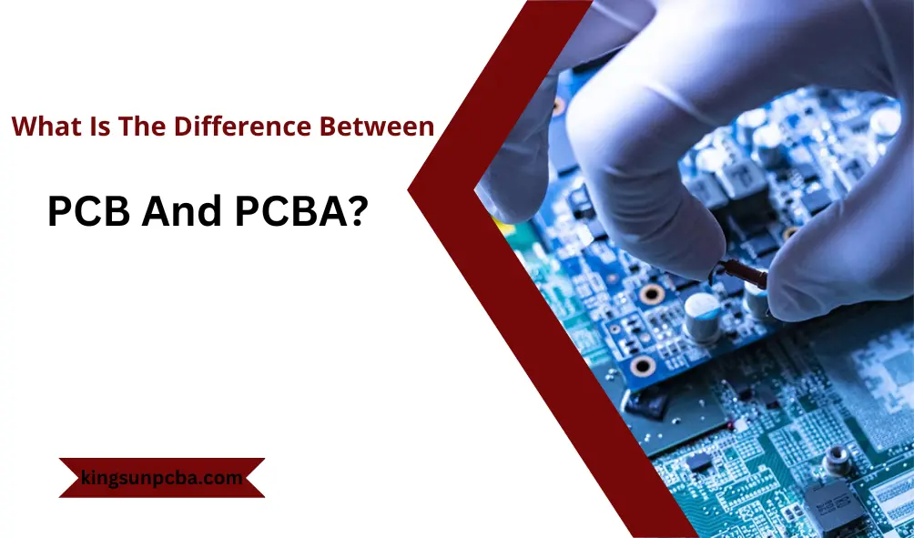
PCB board and PCB assembly are two different terms in the PCB manufacturing industry. However, PCB and PCBA are not the same things in many ways. An audience new to the electronics industry often needs clarification with both terms. Therefore, we have decided to explain the difference very simply.
This article will discuss the difference between PCBA and PCB, including their definition, applications, and advantages.
The advantages of PCB board and PCB assembly include the following:
- Affordable
- High reliability
- Compact size
- Efficient performance
- Quick Turnaround
- Easy repairing
What is a PCB in electronics?
The role of printed circuit boards is to connect, insulate, arrange, and fix electronic components to create circuits, and to transmit signals and power. For example, there are cases in which a high-frequency circuit is created on a printed circuit board and used as an antenna.
These are surface mounted on the board with solder. The surface of a PCB has a coating that protects the copper from corrosion and reduces the chances of short circuit. This coating is called solder resist.
What is PCBA?
PCBA stands for printed circuit board assembly. It refers to assembling electronic components onto a PCB board to create a functional electronic device. The components include:
- Resistors
- Capacitors
- Diodes
- Transistors
- integrated circuits
- and other electronic components
The printed circuit board assembly process involves placing the components onto the PCB, followed by soldering to create a solid mechanical and electrical connection. PCB assembly is used in a wide range of electronic products, including:
- Computers
- Smartphones
- Televisions
- Medical devices
- Automotive electronics
Pcb assembly is essential in creating functional electronic devices. Subsequently, it is critical to the success of the electronics industry.
Next, let’s talk about PCB vs. PCBA.
The Difference Between PCB and PCBA
There are major 3 differences between PCB board and PCB assembly.
- Appearance
- Manufacturing Process
- Manufacturing Cost
1. Appearance
A PCBA is a finished board with all of the electronic components soldered on it, Similarly, a PCB board is a bare circuit. A PCBA is a finished assembly that has every component needed for the board to operate as intended.
2. Manufacturing Process
The manufacturing process PCBs is less complicated compared to PCB assembly. Due to the numerous parts and steps needed in PCB assembly, creating a blank board is a less complicated than manufacturing a finished printed circuit board assembly.
For instance, designing the board, making a photomask, etching the copper traces onto the board, and putting on a solder mask are all common steps in PCB production. On the other hand, PCBA manufacturing includes soldering the components onto the board in addition to all the stages involved in PCB manufacture.
3. PCB cost is significantly less compared to PCB Assembly
Because they are easier to manufacture, PCBs are less expensive than printed circuit board assembly. The kind and quantity of components soldered onto the board have an impact on the price of a PCBA.
Depending on the project need, you start with a bare PCB. Subsequently, you must consult with a professional PCBA manufacturer for PCBA assembly for the mass production.
CBAs are less likely to contain errors than hand-assembled boards. This is because the automated manufacturing processes are very precise and repeatable
Advantages of PCB Board and PCBA
Advantages of Printed Circuit Boards
- With PCB board the miniaturization of electronic devices is simple which enable manufacturers to produce more lightweight and compact products
- PCB boards provides an uninterruptable medium for electronic components. Ultimately, it reduces the risk of signal interference.
- PCB board improves signal transmission and integrity
- Printed circuit board can effortlessly control heath coming from different installed components.
Advantages of PCB Assembly
-
- PCB assembly provides a comprehensive assembly solution. For instance, there is no need to buy and assemble parts separately. This saves time and money.
- Automated production ensures high-quality PCB assembly. This is crucial for medical and industrial equipment performance.
- Due to the smooth automation process of component installation, there are minimum chances of errors in printed circuit board assembly.
PCB Vs. PCBA Manufacturing and Installation Process
The PCB board manufacturing process and PCB assembly are both crucial in terms of cost and efficiency.
Convert CAD data
We edit CAD (Computer Aided Design) data, which has been designed in advance to be used in manufacturing. In addition, the data converted for manufacturing is called CAM (Computer Aided Manufacturing), which is critical information when manufacturing printed circuit boards.
Make a hole in the board
Generally, drilling is performed to create mounting holes, through holes, and mini-via holes on the board. However, this is the manufacturing process’s most time-consuming and costly part. Similarly, we can reduce the cost by increasing the size or reducing the number of holes.
Additionally, with the miniaturization of materials, laser processing has become quite popular in recent years. They are making it possible to perform high-speed and high-quality processing. However, since laser processing uses high-density irradiation energy, it heavily burdens the resin.
Similarly, it is not suitable for processing through holes. Therefore, it is necessary to consider and select the appropriate processing method. Generally, it depends on the type of PCB board and the wiring pattern.
Forming a Copper Foil Pattern
Once the hole-drilling process is complete, copper foil is applied to the entire board to form the pattern. Creating a copper foil pattern requires several steps. Similarly, it is a fundamental process in manufacturing printed circuit boards.
Generally, the process is divided into two steps: exposure and etching, and each procedure is performed using the following steps.
Exposure
Exposure is transferring pattern data converted to CAM onto a substrate. In this process, we use a dry film on a substrate coated with copper foil. Similarly, we apply a photosensitive agent called resist over the dry film. Furthermore, an artwork film with a pattern drawn on it is pasted on top and exposed to ultraviolet light.
Etching
Etching is a method of chemically removing copper foil by spraying chemicals onto the PCB board, etching the exposed substrate, and removing the copper foil from areas other than those covered by the hardened resist.
The copper foil remains in the same shape as the pattern. Finally, by peeling off the dry film using chemicals, we achieve the copper foil pattern according to the design data. For multilayer PCB boards, repeat the same process with an insulating layer crimped in between.
Form solder resist
If the copper foil pattern is left exposed on the board surface, there is no insulating film, and problems will occur. For example, wiring and electronic components will short out. Hence, we apply solder resist to form an insulating film. Its function is to protect the copper foil pattern.
Soldering
Generally, we place the PCB board in a tank of high-temperature molten and solder liquid. Once the entire board is coated with solder liquid, use high-temperature, high-pressure hot air to smooth the solder liquid to a uniform thickness.
This method allows efficient component mounting. Soldering also prevents oxidation of the parts where we mount components and the copper foil.
PCB Assembly Component Installation Process
There are three methods for component installation in PCB assembly. These are:
-
-
- Through-Hole installation
- Mixed Assembly
- Surface Mount Assembly
-
Here, we shall focus on surface mounting assembly process.
1. Solder Paste Printing
In solder pasting, we use a cream solder for printing. We use a jig called a metal mask to separate the areas that require printing. It is to prevent cream solder from being printed on unnecessary areas.
Generally, we use Gerber data to create the metal mask used in this process.
Bond Application
The chip bonding process is a process in which a bond is applied to secure chip components. Its primary role is to fix parts so they do not fall” when mounting components in the flow soldering process.
Another use is to cover extra parts insertion holes with adhesive to prevent manual insertion errors.
Component Installation
This is the process of actually mounting chip components. Chip-mounted components are mainly delivered as reels and then set into cassettes.
By attaching the cassette to the designated location on the mounter, you are ready to mount the component on the PCB board.
2. Reflow oven
This process applies heat to the mounted board to blend the mounted components, chips, and solder.
Each is heated for the following purposes:
-
-
- Cream solder
-
Cream solder is melted by heat and blended with the parts.
-
-
- Chip bonding
-
Cures the bond using heat and fixes the component so it cannot be removed until the mounting process.
The melting temperature of the cream solder and the curing temperature of the chip bond are different.
Therefore, depending on the process, we adjust the temperature to an appropriate temperature and place as little stress on the board as possible.
3. AOI Inspection
The inspection process in PCB assembly is to check the quality of components installed on PCB board. It is a critical step to check potential errors before it goes for reflow soldering. For this process, PCB assembly manufacturers use AOI machines. Similarly, First Assembly Inspection is also important before the product goes into the mass production.
4. Reflow Soldering
Once the surface mounting process is complete, components are manually inserted into the PCB board using a reflow soldering process according to specifications. The major function of this process is to establish a connection between PCB board and all components.
5. Post Flow Inspection
It is the last stage in printed circuit board assembly. The purpose of this visual inspection to ensure that there is no mistake in the product. Now, PCB assembly companies are using 3D technology which can detect such errors significantly.
Summary
The primary difference between PCBs and PCBAs lies in their respective compositions. Printed circuit boards are fully designed boards with wiring patterns. In contrast, PCBAs, are fully assembled boards that incorporate all necessary electronic components.
One prominent distinction is in the manufacturing process of PCBs, which is predominantly carried out in large quantities. Similarly, we can execute PCBAs in either small or large quantities.
Please contact Kingsun PCB, which has 20 years of experience in printed circuit board assembly and provides high-precision, high-quality products and technical know-how.