Introduction
IC (Integrated Circuit) packaging is crucial in the electronics industry. It protects semiconductor components from environmental factors. It also supports their connection and functions within the specific electronic device.
Common IC packaging also includes DIP (Dual Inline Package). How do you define this packaging?
You will explore the role of DIP in the PCB assembly process. You will also learn how DIP compares with other packaging forms used for ICs.
Definition and History of Dual Inline Package
Let’s look at DIP in more detail:
What is Dual Inline Package?
DIP is short for Dual Inline Package. It’s also known as DIL.
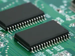
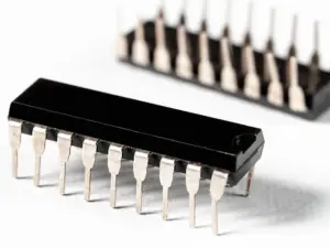
In microelectronics, a dual inline package is a classic integrated circuit package. It has a rectangular casing and two parallel rows of pins for electrical connections.
The pins can be inserted into holes on a PCB (Printed Circuit Board) and soldered. This process is known as through-hole mounting, which makes a strong solder joint. In addition, the DIP can also be inserted into a socket.
History of Dual Inline Package
Three people, Rex Rice, Don Forbes, and Bryant Rogers, invented DIP in 1964. They belonged to Fairchild R&D. The purpose was to deal with the limits of round transistor-style packaging pins.
The inventors made a 14-lead ceramic dual inline package. It had two rows of pins that were 100 mils (0.1 inches) apart. This breakthrough allowed automated insertion into PCBs.
Gradually, the pin count rose to 64 leads (number of pins).
More complex circuits needed more signals to work with complex electronic devices. The invention of the DIP package brought a big advantage. Through it, high-density chip carriers came into being that can easily fix the PCBs.
Applications of Dual Inline Package
DIP packages have been popularly used for a wide range of applications, including:
- Data-processing
- Telecommunication equipment
- Bar graph displays
- Relays
- Light-emitting diodes(LEDs) and resistors
- Transistors and switches
From DIP to SMT
Over time, packaging forms broadened. DIP packages were steadily replaced by SMT packaging. SMT stands for surface mount technology. It’s currently the process used for low-cost, high-production PCB assembly.
Today, SMT is the leading procedure for PCB design in many applications.
SMT packaging has advantages in terms of small weight and size. It also eliminates the cost of extensive drilling and enhances the high interconnection of electronic boards.
SMT components are ideal for mass production but less suitable for circuit prototype production. However, the vast majority of electronics today are made with SMT.
Dual Inline Package Structure
Dual Inline Package (DIP) consists of the following components:
- Lead frame
- silicon die
- package substrate
- polymer mold
- wire bonds of gold
The main component of a DIP is the lead frame. It ensures the electrical connections are complete and holds the silicon die. The lead frame also provides the connecting pins that extend out.
The package substrate is an insulation material that supports the lead frame electrically.
The lead frame has an additional coating of polymer mold. The polymer mold protects the components within the lead frame. It also stops moisture from getting into the lead frame and makes it more reliable.
The silicon die has the electronic circuitry to carry out the required functions. The wire bonds of gold join the lead frame and the silicon die. It allows for flowing electrical signals between the silicon die and the outside world.
Main characteristics of Dual Inline Package
Some important characteristics or features of a DIP package are as follows:
Spacingheat and shock.
JEDEC standards are accepted internationally for DIP packages. According to them, the distance between two pins (pitch) must be 0.1 inches (2.54 mm). The row spacing (distance between two pin rows) depends on the PIN in the package.
Number of Pins
In a DIP package, there is an even number of pins. These are multiples of 2, e.g., 14, 16, 18, and so on. The maximum number of pins used widely in a DIP package could be 52 to 64.
A DIP is typically denoted as DIPn. Here, n is the total number of pins. For example, DIP18 has 18 pins.
Orientation
The position of the notch that identifies the DIP components dictates the pin position.
The notch could be facing up. Thus, the PIN is the first pin on the upper left. The rest are ordered in the anti-clockwise direction.
Suppose a DIP18 package (the number of pins being 18). The identifying notch could be facing up. The left pins are ordered from 1 to 9 from top to bottom. The pins on the right side contain bottom-to-top pins ordered from 10 to 18.
Types of Dual Inline Packages
There are different types of Dual Inline Packages based on size or material:
Plastic dual inline package (PDIP):
It’s the cheapest and most common DIP packaging type; its main material is plastic.
It’s appropriate for a range of integrated circuits. It can save a considerable amount in high-volume and dense assemblies.
Ceramic dual inline package (CDIP)
This package utilizes ceramics instead of plastics. It provides better electrical performance and greater moisture, heat, and shock resistance.
Shrink Plastic dual inline package (SPDIP):
This type of package has a smaller lead pitch of 0.07 in (1.778 mm). That means it reduces by 30%. It’s one of the space-saving options. The pin count on this package ranges from 28 to 64.
Skinny Dual Inline Package (SDIP):
This package is another space-saving option. The pin center distance is 2.54 mm, and the width is 7.62 mm.
Hybrid or Metal DIP
This type of DIP package is made using a combination of metals and other materials.
Pros and Cons of Dual Inline Package
The Dual inline package has several pros and cons, which are as follows:
Pros of DIP
- The DIP package is suitable for through-hole mounting methods, either manually or via automated processes..
- The DIP package is simple in structure with an uncomplicated layout
- DIP package has an easy manufacturing process, which makes them fitting for large production volume.
- DIP package helps to avoid the risk of overheating and allows for heat dissipation.
- DIP packages are reliable as they make a secure connection because of through-hole mounting.
- DIP packages allow for simple troubleshooting, testing, and socketing.
- They are readily replaceable and don’t damage other components.
Cons of DIP
- DIP packages need more space on the circuit boards as opposed to other packaging types.
- The pin spacing of DIP packages may be limited and unfeasible for electronic applications needing high density.
- Temperature changes can result in the expansion or contraction of the pins and badly impact the DIP package.
- DIP packages can get damaged by twisting or bending, thus affecting their toughness as compared to other packages.
Comparison of Dual Inline Package with other packaging forms
Dual Inline Package (DIP) and Small Outline Integrated Circuit (SOIC) are two packaging forms. These are typically used for integrated circuits (ICs). In addition, there’s also a single inline package (SIP), an IC package that is not as common as the dual inline package (DIP).
An SOIC is a surface-mounted IC that has an area of about 30-50% less than an equivalent Dual Inline Package.
The following table compares the chief differences between DIP packages, SOIC packages, and SIP packages:
| Property or characteristic | Dual Inline Package (DIP) | Single Inline Package (SIP) | Small Outline Integrated Circuit (SOIC) |
| Number of rows of pins | Two | Single | Two |
| Pitch (distance between two pins) | 0.1 inches (2.54 mm) | 0.1 inches
(2.54 mm) |
0.5 mm to 1.27 mm |
| Number of pins | Up to 64 pins | Up to 24 pins | Up to 48 pins |
| Through-Hole Mounting | Yes | Yes | No |
| Surface Mounting | No | No | Yes |
| Size | Bigger than SOIC | Smaller than DIP | Smaller than DIP |
| Pin (Lead) Count | Even | Even | Even or odd |
| Pin (Lead) position | Inline | Inline | J-lead and Gull-wing |
| Price | Lower than SOIC | Lower than DIP | Higher than DIP |
| Electrical Performance | Worthwhile | Worthwhile | Better than SIP and DIP |
| Suitability for SMT applications | Less Suitable | Less Suitable | More Suitable |
Conclusion
Indeed, surface mount technology (SMT) has increasingly replaced Dual Inline Packaging today. However, DIP remains highly suitable for PCB prototyping, product development, and education.
To recap, DIP packages are known for being low-cost, simple, and compatible with through-hole mounting technology.
Thus, you can better decide that this detailed DIP package guide will help you choose the right packaging form for your next electronic project.