Understanding PCB vias, the essential elements for connecting layers within a PCB, is crucial for high-performance design.
This guide dives into basics like pad and drill sizes and manufacturer capabilities. We’ll explore via placement strategies to minimize inductance, improve assembly, and avoid voids. We’ll also cover stitching PCB vias for shielding purposes.
What is a Via?
We all know traces are connections on a plane. So, on a layer, we can route anywhere on that plane, usually called a trace. Or we can use things such as copper pours.
However, we must use a via once we want to route between layers, such as connecting layer one to layer three.
Essentially, it’s just a vertical connection in the third dimension. It is used for connections between layers, so our trace on one layer can jump to any or multiple layers in a PCB. We don’t just have to end up on one layer.
If we’re not connecting to a specific layer via a link, we will create a void on that layer, and we’ll look at that in more detail later.
Types of Vias
Printed circuit boards are stacked with copper foil circuit layers, with vias connecting between different circuit layers. The drill cost can be up to 30%-40% of the entire board.
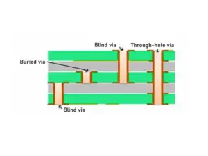
Plated through hole (PTH), blind hole (BVH), and buried hole (BVH) are the standard types in PCB design vias. The details of these three types of substrate via holes are shown below.
Plated through hole (PTH)
Plated through-holes are the most common PCB vias. If you face the board to the light and see the light, it’s a “through hole.” Incorporating a laser will significantly assist you in making a complete borehole.
Furthermore, the cost will be relatively low. However, in some cases, no through holes are required. It’s cheaper, but it may need more board space.
There are usually two types of through holes: PTH and NPTH. The difference between the two is whether it has copper or not.
PTH holes do not have copper and are often used for inserting electronic components (the hole diameter is slightly larger). It is also used to connect patterns on the inner and outer layers.
Blind Beer Hall (BVH)
Unlike through-hole vias that pass entirely through the PCB, blind vias connect the outermost layer and a single, specific inner layer.
Since the via doesn’t emerge on the opposite side of the board, it’s called a “blind path.” This technique allows for more efficient use of space on the PCB’s surface.
This manufacturing method requires attention to the hole depth (Z-axis). Because hole plating is complex, only some board manufacturers use this method.
Buried via hole (BVH)
A buried via hole is a hole that connects to any circuit layer on the board without passing through the outer layer.
This process cannot be carried out using the method of drilling and bonding but requires the drilling process to be made into individual circuit layers, followed by plating and then lamination pressing, which are repeated in three steps.
It takes longer to manufacture than “through hole” and “blind via hole,” and its price is the highest.
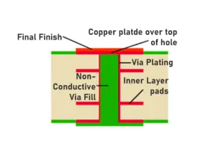
HDI PCBs often incorporate blind vias to maximize space for additional circuit layers. Besides drill sizes, pad sizes, and annular rings, many other parameters make up a via.
For example, PCB via tenting, which covers the via with the solder mask, typically costs no extra; filling the via will be additional.
What are the differences between the various types of vias?
One can be sure through-hole vias were made with a drill. Different drill sizes are used, but generally, nothing less than 0.2 mm is used. They go up from there to very much bigger ones.
The drills make the holes under digital control using numerically controlled machines.
As a general rule, multi-spindle tools are used. Subsequently, the tiny holes are made in batches, one after the other. It takes a finite time, and linear motors control the spindles. They turn relatively fast to achieve a good hole quality.
Functionality of Vias
When we’re talking about vias, we have specific main parameters. PCB vias are critical in accelerating complex functions on a layered PCB. Let’s explore each:
Signal Routing:
Without through-hole vias, signals could not travel from one layer of the PCB to another. Vias’ role is similar to that of electrical lifts, as they help provide interconnection between different layers. Therefore, this allows the designers to have complex networks and ensure fast signals are effectively transmitted.
Power and Ground Distribution:
Vias are crucial for delivering power and ground throughout the PCB. They connect power and ground planes on different layers. Subsequently, they ensure a stable and consistent voltage supply to all components. In addition, PCB vias minimize voltage drops and maintain signal integrity.
Escape Routing:
Surface mount technology (SMT) has leads. These leads need to connect to internal layers. Vias, particularly through-hole vias, provide an escape route for these connections.
What are the rules for routing a PCB?
This is very important. Let’s talk about the routing rules for through holes. According to the IPC standards, a hole must be centered on the pad. According to the IPC and ISO, a hole at a tangent to the pad is allowed, but the printed circuit board material can move, and machines have a tolerance. For these reasons, the pad must be larger than the hole diameter.
If you take the example of a pad of 0.55 mm, you can drill a hole of 0.3 mm. This will give us a finished hole between 0.2 and 0.25 mm, which is relatively small. Similarly, in this case, we must allow isolation on the internal layers of the order of 750 µ if we don’t want a connection.
Also, externally, we need a center opening in the varnish of around 450 µ. It is about 1/2 more than the drilled diameter. Regarding laser micro vias, at the PCB design level, the standard is to have a pad of 300 µ. Here, the finished hole will be around 100 µ. In this case, we can go a little tighter to a minimum of 275. So remember that laser vias offset from the pads of the BGA.
How do I choose the via in my PCB design?
It isn’t easy to give general via diameters and parameters you should always use. It depends on the scenario you’ll need. If you’re routing out a very fine-pitch BGA, your via needs will be completely different from routing out an audio through-hole board.
We have to take some things into account, though. A small drill size, for example, something like 0.15 millimeters or anything less than 0.2 millimeters, will typically give an increased PCB cost and a lower yield.
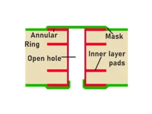
Via Parameters
This term refers to the size and conduct of the hole. It consists of pad size (overall diameter of the hole), drill size (the actual size of the hole), and annular ring (hole’s space from a pad).
Their manufacturer capabilities determine the least drill size and ring width they can produce reliably.
Via Placement:
Where you position your vias is essential! Proper choice will reduce inductance (electrical resistance), which can affect signal integrity at high frequencies.
It also guarantees components that can be adequately soldered in assembly and adds to it.
It also helps avoid “voids”- these refer to unoccupied areas on a substrate that might weaken it.
Via Types
There is not just one kind of via! Through-hole vias are prevalent types crossing the entire board.
Blind vias only connect inner layers with themselves without going up to the surfaces of PCBs.
On the other hand, Buried vias do not go through to any external layers but are located between internal layers only. Microvias are small holes found on high-density printed circuit boards (PCBs).
The decision regarding via type entirely depends on PCB design requirements.
Via Sizing
Via sizing involves trade-offs. Smaller vias may save space but increase manufacturing costs and yield higher inductance values; Larger ones take more space but are more accessible for manufacturers.
These general recommendations provide some guidance. However, the best size depends on what you want your application for.
Again, it depends entirely on the scenario. But I often get asked this question: “What via size do you recommend?” And as a general starting point, this seems about right.
When talking about vias, we also need to think, as with traces, about the current handling capabilities.
Conclusion
In conclusion, vias are decisive in the building blocks of any complex printed circuit board.
We have tried to provide various types, parameters, and placement strategies for designing high-performance electronics.
Learning about vias helps create complex connections and bring your PCB designs to life.