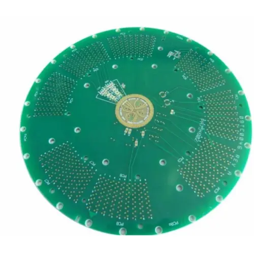
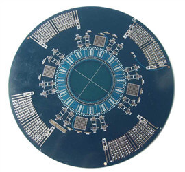
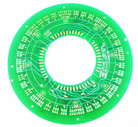
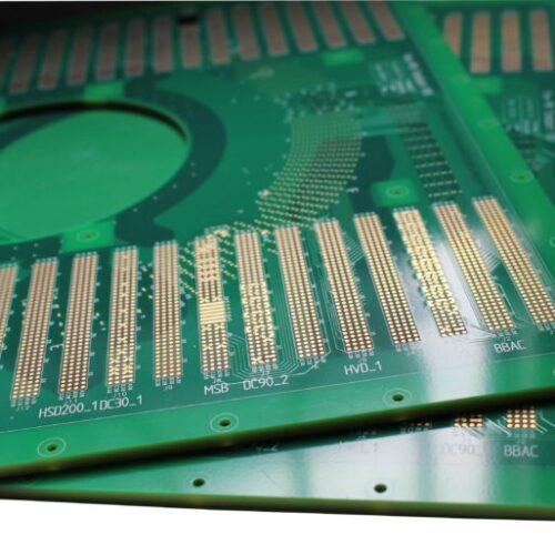
Via in pad PCB with Gold Plating
- Layers: 4 Layer
- PCB Material: FR4 TG170
- Board Thickness: 1.6mm
- Surface Finishing: Hard gold 30 microinch plating
- Finished Copper thickness: 1/1/1/1 OZ
- Solder mask: Green color
Special Process:
Our Service:
- Quickturn around PCB prototype manufacturing
- PCB fabricate and PCB assembly service
- Stencil service
| Minimum Circuit Trace Width/Space: 2.7/2.7mil |
| The Minimum Via Size: 0.15mm |
| The Minimum legend Height/Width: 0.5mm/0.12mm |
| Surface Finishing: HASL-LF, ENIG, ENEPIG, OSP, Gold Finger, Hard Gold Plating, Immersion Silver, Immersion Tin |
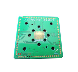
| Special Technology: Blind&buried via, Via In Pad, Backdrill, Small BGA Pad, Impedance control, Heavy Copper, Copper Filled Vias, Countersink hole, Depth Milling |
| Material Type: FR4,Metal Core,Halogen Free FR4,Rogers,PTFE,Arlon,Nelco,Polyimide |
| Final Board Thickness: 0.4mm ~ 6.0mm |
| Final Copper Thickness: HOZ 1OZ 2OZ 3OZ 4OZ 6OZ 10OZ |
| FR4 Substrate Thickness: 0.1mm 0.2mm 0.3mm 0.4mm 0.5mm 0.6mm 0.8mm 1.0mm 1.2mm 1.5mm 2.0mm 2.36mm |
| Shaping: CNC Routing, Punching, V-CUT, Depth milling, Castellation |
| Special Hole: Blind&buried hole, Depth milling, T-slot, Countersink hole |
| Quick-turn Lead Time: 1 Day for 2 Layer PCB, 2 Days for 4 Layer PCB, 3 Days for 6 Layer PCB |
-gallery-770x578-1-500x500.jpg)